A growth method of organic single crystal microribbon p-n heterojunction array

A growth method and micro-belt technology, which is applied in single crystal growth, single crystal growth, crystal growth, etc., can solve the problems of difficult to control the accurate growth of upper layer materials, and the inability to accurately locate single crystal materials, etc.

Active Publication Date: 2019-08-30
苏州英凡瑞得光电技术有限公司
View PDF4 Cites 0 Cited by
  • Summary
  • Abstract
  • Description
  • Claims
  • Application Information

AI Technical Summary

Problems solved by technology

However, this method is difficult to control the accurate growth of the upper layer of material on the pre-built first layer of material, in other words, this method cannot accurately position the growth of the upper layer of single crystal material

Method used


Image

  • A growth method of organic single crystal microribbon p-n heterojunction array
  • A growth method of organic single crystal microribbon p-n heterojunction array
  • A growth method of organic single crystal microribbon p-n heterojunction array

Examples


Embodiment Construction

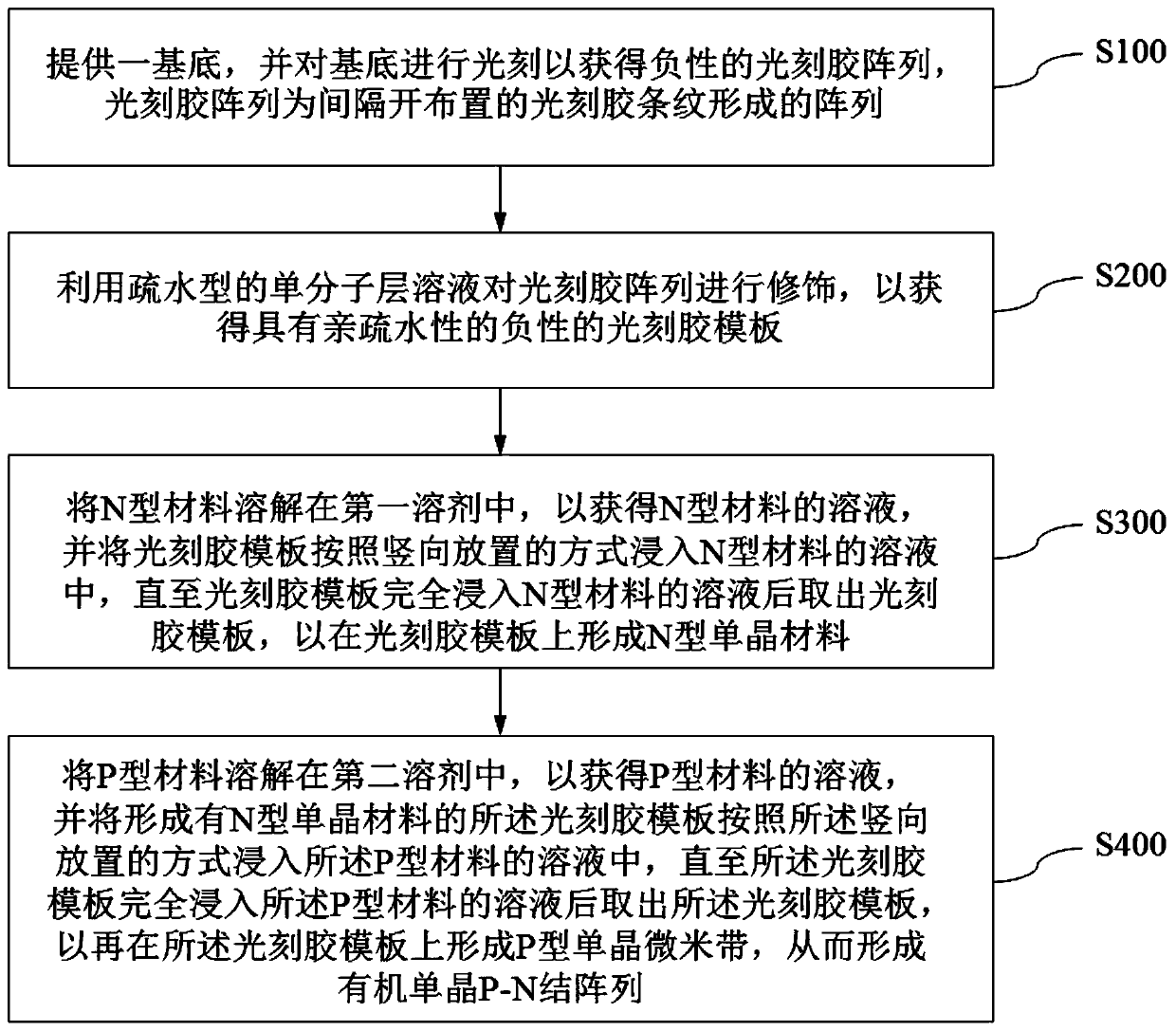
[0031] figure 1 It is a schematic flowchart of a method for growing an organic single crystal microbelt P-N heterojunction array according to an embodiment of the present invention. Such as figure 1 As shown, the growth method includes the following steps:

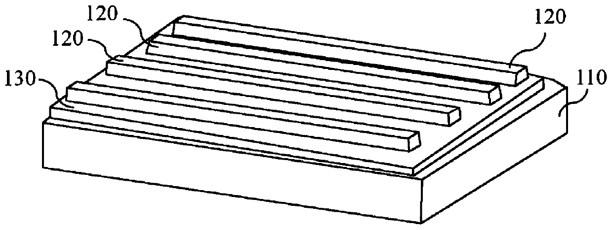
[0032] S100. Provide a substrate, and perform photolithography on the substrate to obtain a negative photoresist array. The photoresist array is an array formed by a plurality of photoresist stripes arranged at intervals;

[0033] S200: Use a hydrophobic monolayer solution to modify the photoresist array to obtain a negative photoresist template with hydrophilicity and hydrophobicity;

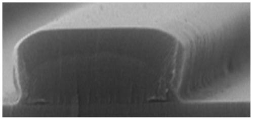
[0034] S300. Dissolve the N-type material in the first solvent to obtain a solution of the N-type material, and immerse the photoresist template in the solution of the N-type material in a vertical manner until the photoresist template is completely immersed in the N-type material. After the material solution, the photoresist template is taken ou...


PUM


Abstract

The invention provides a growth method of an organic monocrystal micro-strip P-N heterojunction array. The method comprises the steps that a substrate is provided, and photoetching is conducted on thesubstrate to obtain a negative photoresist array; the negative photoresist array is modified through a hydrophobic monomolecular layer solution to obtain a photoresist template; the photoresist template is vertically soaked into an N type material solution till the photoresist template is completely immersed into the N type material solution, then the photoresist template is taken out, and an N type monocrystal micro-strip is formed on the photoresist template; the photoresist template is vertically soaked into a P type material solution till the photoresist template is completely immersed into the P type material solution, then the photoresist template is taken out to form a P type monocrystal micro-strip on the photoresist template, and then the organic monocrystal micro-strip P-N heterojunction array is formed. The prepared micro-strip P-N heterojunction array is a monocrystal material, and accurate orientation growth of P-N heterojunctions of an up-down stacked structure can be achieved.

Description

Technical field [0001] The present invention relates to the field of semiconductor technology, in particular to a method for growing an organic single crystal microbelt P-N heterojunction array. Background technique [0002] Organic single crystal semiconductor has a highly ordered molecular arrangement. This structural feature makes it have a high carrier mobility, so it has a wide range of potential applications in organic circuits. Currently, there are many methods for patterning or arraying organic single crystals, such as inkjet printing, solution coating, and self-assembly through templates. It is reported that the mobility of organic single crystals patterned or arrayed by these methods can exceed 10 cm 2 V -1 s -1 . However, most of these organic materials have only unipolar properties such as P-type or N-type, which affects their application in complementary metal oxide semiconductor circuits (CMOS circuits) and new devices such as light-emitting transistors. [0003] CM...

Claims


Application Information

Patent Timeline
Patent Type & Authority Patents(China)
IPC IPC(8): C30B29/54C30B7/00H01L21/8238
Inventor 张秀娟张晓宏揭建胜邓巍茆健
Owner 苏州英凡瑞得光电技术有限公司
Why Eureka
Try Eureka