Density functional and hybrid functional-based method for calculating defect motion of Si

A technology of density functional and hybridization, applied in the field of analog calculation, can solve the problem of low accuracy of Si movement energy, achieve the effect of improving calculation accuracy, less time-consuming, and lower cost

Active Publication Date: 2018-07-31
HARBIN INST OF TECH
View PDF2 Cites 4 Cited by
  • Summary
  • Abstract
  • Description
  • Claims
  • Application Information

AI Technical Summary

Problems solved by technology

[0004] The purpose of the present invention is to solve the problem of low accuracy of obtaining the defect movement energy of Si by using the density functional method, and provide a method for calculating the defect movement of Si based on density functional and hybrid functional

Method used


Image

  • Density functional and hybrid functional-based method for calculating defect motion of Si
  • Density functional and hybrid functional-based method for calculating defect motion of Si
  • Density functional and hybrid functional-based method for calculating defect motion of Si

Examples


specific Embodiment approach 1

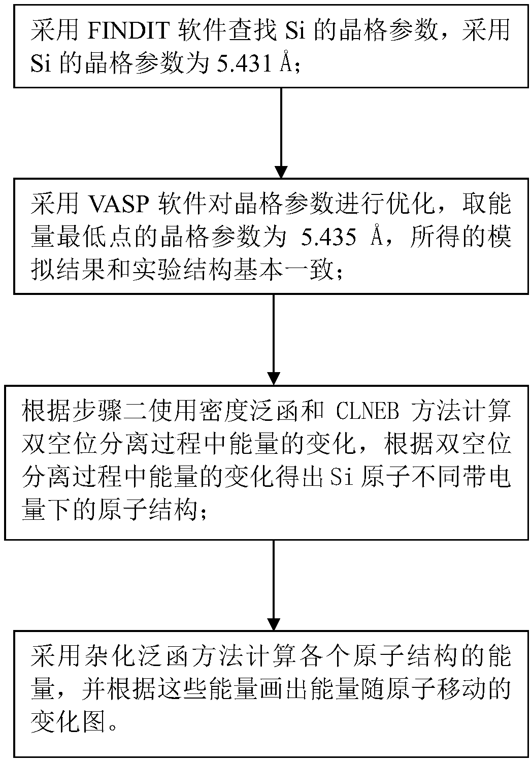
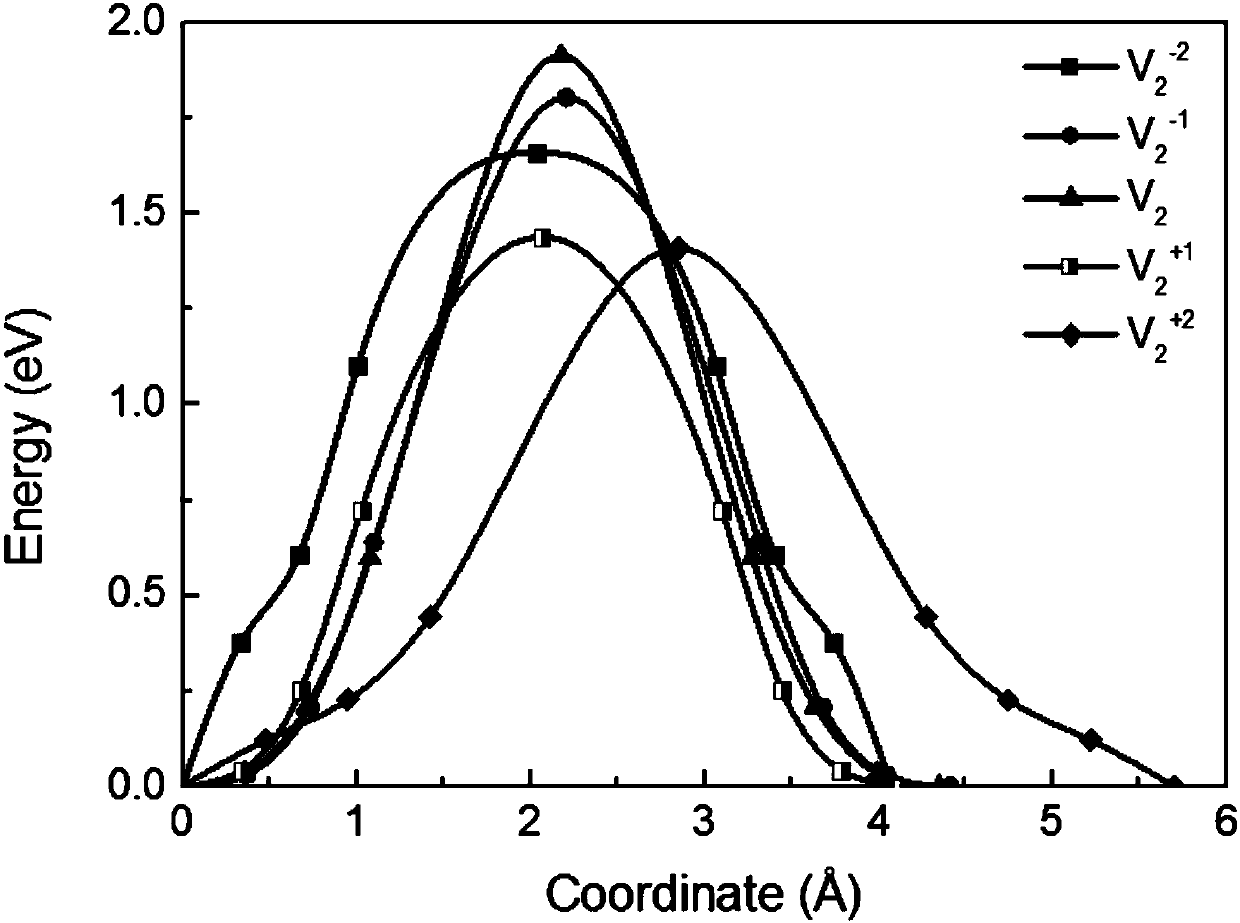
[0028] Specific implementation mode one: combine figure 1 To illustrate this embodiment, the specific process of the method for calculating the defect movement of Si based on density functional and hybrid functional in this embodiment is as follows:

[0029] Step 1: use FINDIT software to find the lattice parameters of Si, and obtain the lattice parameters of Si, that is, the experimental results are α=90°, β=90°, γ=90°;

[0030] a is the unit cell side length parameter of the lattice, b is the unit cell side length parameter of the lattice, c is the unit cell side length parameter of the lattice, and α, β, γ are the three angle parameters of the unit cell of the lattice;

[0031] Literature search for the forbidden band width of Si lattice, the forbidden band width is 1.2eV;

[0032] (The literature is C. Janowitz, V. Scherer, M. Mohamed, A. Krapf, H. Dwelk, R. Manzke, Z. Galazka, R. Uecker, K. Irmscher and R. Fornari / / New or J. Phys. 13 (2011) 085014. PHYSICAL REVIEW ...

specific Embodiment approach 2

[0043] Specific embodiment two: the difference between this embodiment and specific embodiment one is: adopt VASP software to optimize the crystal lattice parameter of Si in the described step two, concrete process is:

[0044] Let all the plane wave cutoff energy of Si be 320eV, the K point be 1×1×1, the Si electron convergence precision be 1E-5, and the Si ion convergence precision be 1E-2. The lattice parameter simulation result of the lowest Si energy point is α=90°, β=90°, γ=90°.

[0045] Other steps and parameters are the same as those in Embodiment 1.

specific Embodiment approach 3

[0046] Specific embodiment three: the difference between this embodiment and specific embodiment one or two is: the corresponding data (a and a ratio, b and b ratio, c and c ratio, α and α Ratio, β to β ratio, γ to γ ​​ratio, the difference between 3%-10%, and satisfying the forbidden band width is equal to the forbidden band width of the lattice of Si searched in step 1, it is considered that the simulation results are consistent with the experimental results.

[0047] Other steps and parameters are the same as those in Embodiment 1 or Embodiment 2.


PUM


Abstract

The invention discloses a density functional and hybrid functional-based method for calculating a defect motion of Si, relates to a method for calculating the defect motion of the Si, and aims to solve the problem of low accuracy of obtaining defect motion energy of the Si by adopting a density functional method at present. The method comprises the steps of obtaining a lattice parameter of the Si;obtaining a lattice parameter of an energy minimum point of the Si; according to the lattice parameters and the band-gap width, obtaining a simulative result consistent with an experimental result; calculating energy change in a bivacancy separation process by using density functional and CLNEB methods, obtaining atomic structures of Si atoms under different electrified capacity, and calculatingthe energy change in the bivacancy separation process by adopting a hybrid functional method according to the structures. The method is used in the field of Si defect motion calculation.

Description

technical field [0001] The invention relates to a method for calculating defect movement of Si, belonging to the field of simulation calculation. Background technique [0002] With the rapid development of modern microelectronics technology, silicon is the most important and widely used material. Since Si is the most critical part of electronic devices, when it is applied in our life and aviation, its reliability will affect the normal application of the whole system. Especially for the space environment, it is often full of various charged particles and rays. When semiconductors are irradiated with these particles or rays, defects inevitably arise. Defects will introduce defect energy levels, reduce the minority lifetime and mobility, and then affect the performance of the device. After investigation, double vacancies are regarded as the most important and common defect, and this kind of defect is easy to move, so it is necessary to investigate the movement of this kind ...

Claims


Application Information

Patent Timeline
Patent Type & Authority Applications(China)
IPC IPC(8): G06F19/00
CPCG16C20/20
Inventor 李兴冀刘超铭魏轶聃杨剑群董尚利
Owner HARBIN INST OF TECH
Why Eureka
Try Eureka