Vacuum absorbing template for semiconductor wafer polishing device and polishing device

A technology of vacuum adsorption and polishing device, which is applied to surface polishing machine tools, grinding/polishing equipment, grinding workpiece supports, etc., can solve the problems of complex polishing process, environment cost, time-consuming and labor-intensive, and reduce production costs. , Improve the yield and thickness uniformity, and shorten the processing time.

Pending Publication Date: 2018-08-03
THE 13TH RES INST OF CHINA ELECTRONICS TECH GRP CORP
View PDF6 Cites 6 Cited by
  • Summary
  • Abstract
  • Description
  • Claims
  • Application Information

AI Technical Summary

Problems solved by technology

[0005] In order to solve the technical problems of complicated wafer polishing process, heavy pollution, high cost and time-consuming and labor-consuming, the present invention provides a vacuum adsorption template for a semiconductor wafer polishing device and a device containing the template, which adopts an improved ceramic disc structure, A vacuum suction cup with a visor structure is added between the ceramic plate and the wafer, and the technical scheme of vacuum adsorption and positioning of the wafer is connected to the vacuum generating structure through the through hole, which realizes the firm positioning of the five-sided wrapping of the wafer, and comprehensively protects the upper surface of the wafer and At the same time, it is convenient for rapid polishing processing, which improves the yield and thickness uniformity, avoids pollution, and reduces costs.

Method used


Image

  • Vacuum absorbing template for semiconductor wafer polishing device and polishing device
  • Vacuum absorbing template for semiconductor wafer polishing device and polishing device
  • Vacuum absorbing template for semiconductor wafer polishing device and polishing device

Examples


Embodiment 1

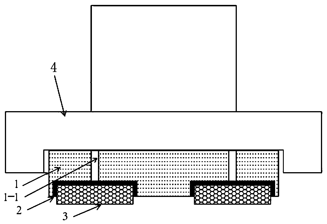
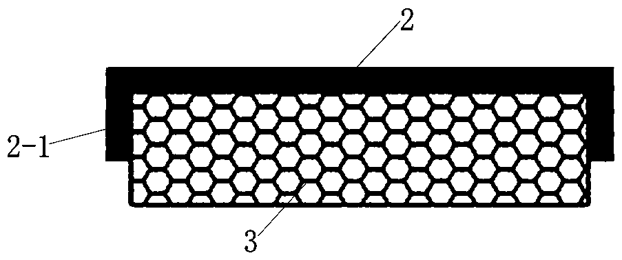
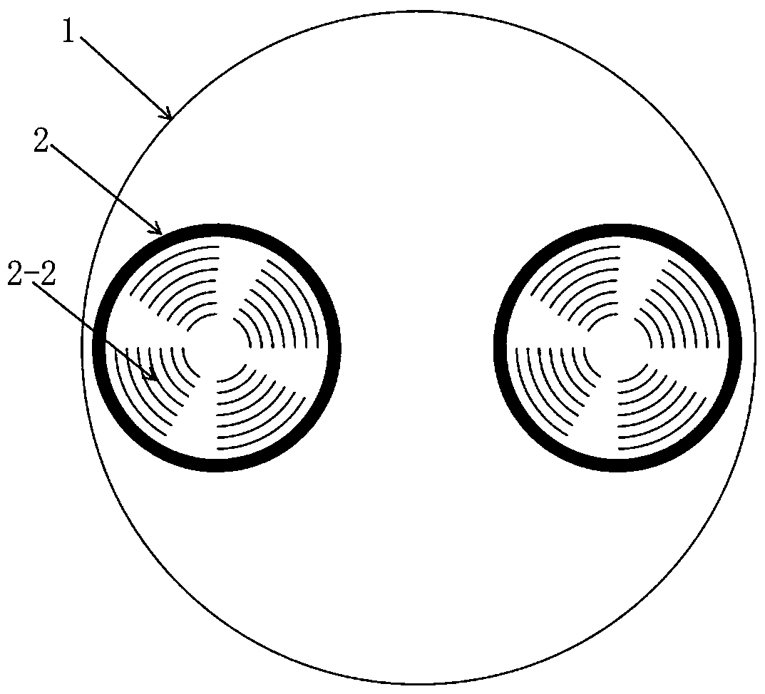
[0024] This embodiment provides a vacuum adsorption template for a semiconductor wafer polishing device, which is used to position the wafer 3 so as to realize single-sided polishing of the wafer 3, see Figure 1-3 As shown, the vacuum adsorption template includes a ceramic disc 1 positioned on the polishing head 4. The key design of this embodiment is that a groove is provided on the surface of the ceramic disc 1, and the shape of the groove is consistent with the shape of the wafer 3 to be polished. , if it can be square or other, it is cylindrical in the present embodiment; the number of grooves on the surface of the ceramic disc 1 can be customized according to the actual situation, and there are 2 in the present embodiment; a vacuum suction cup 2 is positioned in the groove , the positioning method is vacuum adsorption, the peripheral edge of the vacuum chuck 2 extends downward to form a visor 2-1 structure, because the peripheral edge extends downward, the middle part for...

Embodiment 2

[0029] The difference from Embodiment 1 is that in this embodiment, the vacuum suction cup 2 is bonded in the groove of the ceramic disc 1 to achieve positioning. If replacement is required, remove the vacuum and replace the ceramic disc 1 to achieve.

[0030]Put the InP wafer into the common porous ceramic vacuum adsorption template and the vacuum adsorption template described in the above-mentioned embodiment 1 respectively, and perform single-sided polishing. Under the same vacuum negative pressure, the vacuum adsorption template described in the embodiment 1 absorbs Strong force, firm adsorption, no shedding phenomenon, no scratches and wear on the side and the adsorbed surface; while the shedding rate of ordinary porous ceramic vacuum adsorption templates is higher than 30%, and the occurrence rate of side scratches or scratches on the adsorbed surface is higher than 30%; Slightly increase the vacuum negative pressure, the wafer packed into the vacuum adsorption template o...


PUM


Abstract

The invention provides a vacuum absorbing template for a semiconductor wafer polishing device and a polishing device, and belongs to the technical field of wafer polishing. The vacuum absorbing template for the semiconductor wafer polishing device comprises a ceramic disc positioned on a polishing head; a groove is formed in the disc surface of the ceramic disc; a vacuum sucker is positioned in the groove; the peripheral edge of the vacuum sucker downwards extends to form a cap edge structure; and a groove is formed in the inner surface of the vacuum sucker, and is connected with a vacuum generation structure by dint of a vacuum hole penetrating through the ceramic disc for vacuum absorption positioning of wafers. The vacuum absorbing template for the semiconductor wafer polishing device has the following beneficial effects: such process links as wax bonding and wax removal are saved, so that the machining time is shortened, and the pollution is prevented; the cap edge structure achieves an anti-scratch protecting effect on the wafers, so that the vacuum absorbing template is more suitable for polishing of semiconductor wafers with lower hardness and formed by such volatile elements as Si, Ge, GaAs and InP; and the vacuum absorbing template achieves a stable positioning maintenance effect on the wafers, improves the yield and the thickness uniformity, and reduces the productioncost.

Description

technical field [0001] The invention relates to the technical field of wafer polishing, in particular to a vacuum adsorption template and a polishing device for a semiconductor wafer polishing device, especially suitable for VGF crystal growth of semiconductor crystal materials such as indium phosphide and gallium phosphide that need to be synthesized with volatile elements . Background technique [0002] Nowadays, the application range of semiconductor materials is more and more extensive, including computers, electronic devices, optical fiber communications, etc., and semiconductor materials are playing an important role. Such as Si, Ge, III-V compound semiconductor materials and so on. In the technical field of material preparation, single-side polishing of wafers is an important process link. At present, most of the single-side polishing processes use solid wax or liquid wax to stick the wafer to the polishing disc, then perform the polishing process on a single polish...

Claims


Application Information

Patent Timeline
Patent Type & Authority Applications(China)
IPC IPC(8): B24B29/02B24B41/06
CPCB24B29/02B24B41/06
Inventor 王阳孙聂枫孙同年
Owner THE 13TH RES INST OF CHINA ELECTRONICS TECH GRP CORP
Why Eureka
Try Eureka