Short circuit robustness improvement IGBT (insulated gate bipolar transistor) and preparation method thereof

A robust and consistent technology, applied in circuits, semiconductor/solid-state device manufacturing, semiconductor devices, etc., can solve the problems of rapid IGBT failure, improve breakdown voltage, improve short-circuit survival time and robustness, and reduce leakage The effect of current

Active Publication Date: 2018-08-17
ANHUI UNIVERSITY OF TECHNOLOGY
View PDF7 Cites 0 Cited by
  • Summary
  • Abstract
  • Description
  • Claims
  • Application Information

AI Technical Summary

Problems solved by technology

[0007] Aiming at the problem of rapid failure of IGBT in short circuit in the prior art, the present invention proposes an IGBT with improved short circuit robustness and a preparation method thereof

Method used


Image

  • Short circuit robustness improvement IGBT (insulated gate bipolar transistor) and preparation method thereof
  • Short circuit robustness improvement IGBT (insulated gate bipolar transistor) and preparation method thereof

Examples


Embodiment 1

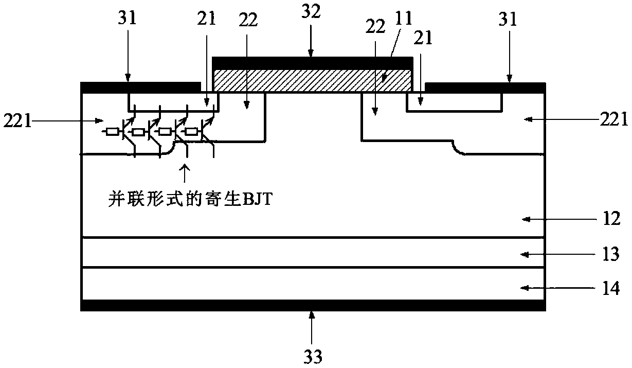
[0047] combine figure 2 , an IGBT with improved short-circuit robustness in this embodiment, comprising an emitter region 21 doped with a second conductivity type, a base region 22 doped with a first conductivity type and a semi-insulating region 222, and a doped region with a second conductivity type The emitter region 21 is located on top of the semi-insulating region 222 , and the base region 22 doped with the first conductivity type is located at the side of the emitter region 21 and the semi-insulated region 222 doped with the second conductivity type.

[0048] The existence of the semi-insulating region 222 reduces the area where the parasitic BJT exists, that is, reduces the number of parasitic BJTs, but there are still a small amount of parasitic BJTs under the channel region, but due to the great reduction in the number of parasitic BJTs, thereby reducing The leakage current in the IGBT during a short circuit reduces the operating temperature, and the time for the IG...

Embodiment 2

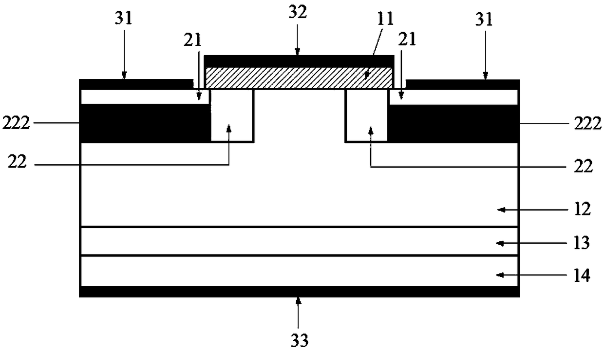
[0053] combine figure 2 , an IGBT with improved short-circuit robustness in this embodiment is further improved on the basis of Embodiment 1. The depth of the base region 22 doped with the first conductivity type is the same as the depth of the emitter region 21 doped with the second conductivity type and the half The sum of the heights of the insulating regions 222 is equal.

[0054] Precisely control the effective width of the conductive channel formed by the base region 22 doped with the first conductivity type, which will not change due to the introduction of the semi-insulating region 222, and ensure the threshold voltage, on-resistance, transconductance, output characteristics, etc. of the IGBT The parameters do not change due to the introduction of the semi-insulating region 222 . While not affecting the IGBT channel region, it can not only improve the short-circuit survival time and robustness of the IGBT, but also increase the breakdown voltage of the IGBT, killing ...

Embodiment 3

[0056] combine figure 2 In this embodiment, an IGBT with improved short-circuit robustness is further improved on the basis of Embodiments 1 and 2. The width of the emitter region 21 doped with the second conductivity type is consistent with the width of the semi-insulating region 222 . The width ratio of the base region 22 doped with the first conductivity type and the emitter region 21 doped with the second conductivity type is 1:1-3. In specific applications, you can choose 1:1; 1:2; 1:3; 1: 1.5 and other values.

[0057] Ensure that the effective channel length of the IGBT does not change due to the introduction of the semi-insulating region 222 , and ensure that parameters such as the threshold voltage, on-resistance, transconductance, and output characteristics of the IGBT do not change due to the introduction of the semi-insulating region.


PUM


Abstract

The invention belongs to the technical field of high-voltage power electronics and discloses a short circuit robustness improvement IGBT (insulated gate bipolar transistor) and a preparation method thereof. The IGBT comprises a second conduction type doped emitter region, a first conduction type doped base region and a semi-insulating region. The second conduction type doped emitter region is positioned at the top of the semi-insulating region, and the first conduction type doped base region is positioned on one side of the second conduction type doped emitter region and the semi-insulating region. The semi-insulating region is formed by steps including ion implantation of second conduction type impurities to realize contra-doping to form an electric neutral layer and ion implantation of amphiprotic impurity elements to form the semi-insulating region. By reduction of an existence region of IGBT parasitic transistors, the problem of 'hot rush' caused by current control failure resultedfrom starting of conventional IGBT parasitic transistors under a short circuit condition is solved, robustness of the IGBT in a short circuit state can be remarkably improved, short circuit resistingtime and critical short circuit energy of the IGBT are increased, and breakdown voltage of the IGBT is raised appropriately.

Description

technical field [0001] The invention relates to the technical field of high-voltage power electronics, in particular to an IGBT with improved short-circuit robustness and a preparation method thereof. Background technique [0002] With the continuous improvement of the performance requirements of power conversion devices, higher requirements are put forward for the IGBT devices that undertake the power conversion function. One of them is that the IGBT devices that undertake the power conversion function should have a certain resistance Short-circuit capability, that is to say, has high robustness. Before the protection circuit can intervene, the IGBT can bear high current stress under short-circuit conditions for a short time. Therefore, the robustness under short-circuit conditions reflects the performance of IGBTs. one of the important indicators. [0003] The study found that there is a natural parasitic transistor (BJT) in the IGBT body, and this BJT is composed of fig...

Claims


Application Information

Patent Timeline
Patent Type & Authority Applications(China)
IPC IPC(8): H01L29/739H01L21/331
CPCH01L29/66333H01L29/7395H01L29/0653H01L29/66068H01L29/1608H01L29/7802
Inventor 周郁明王兵
Owner ANHUI UNIVERSITY OF TECHNOLOGY
Why Eureka
Try Eureka