Inflection point-based HDR image sensor pixel structure and imaging system
An image sensor and pixel structure technology, applied in the field of image sensors, can solve the problem that the pixel structure cannot support multiple exposure modes, and achieve high dynamic range characteristics and prevent overexposure.
- Summary
- Abstract
- Description
- Claims
- Application Information
AI Technical Summary
Problems solved by technology
Method used
Image
Examples
Embodiment 1
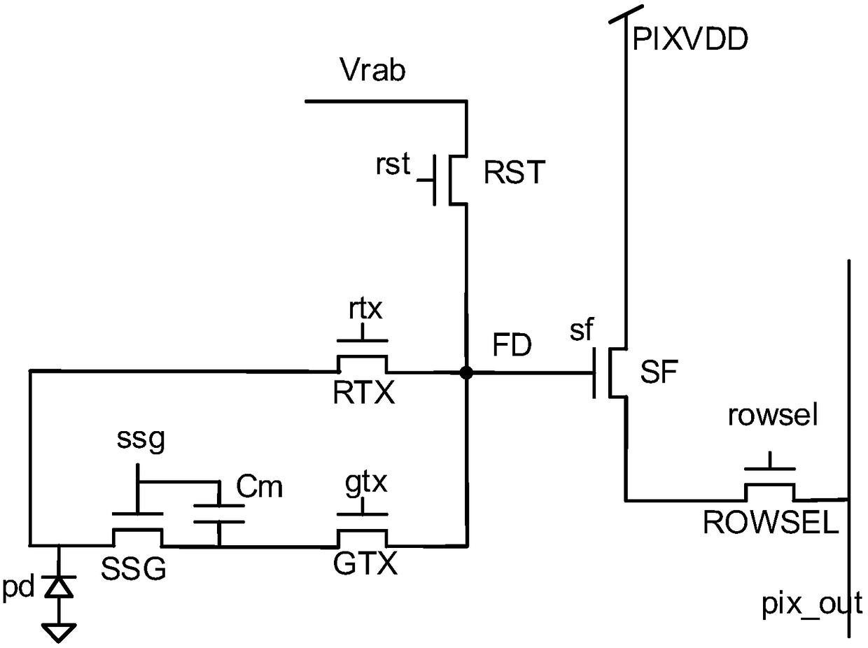
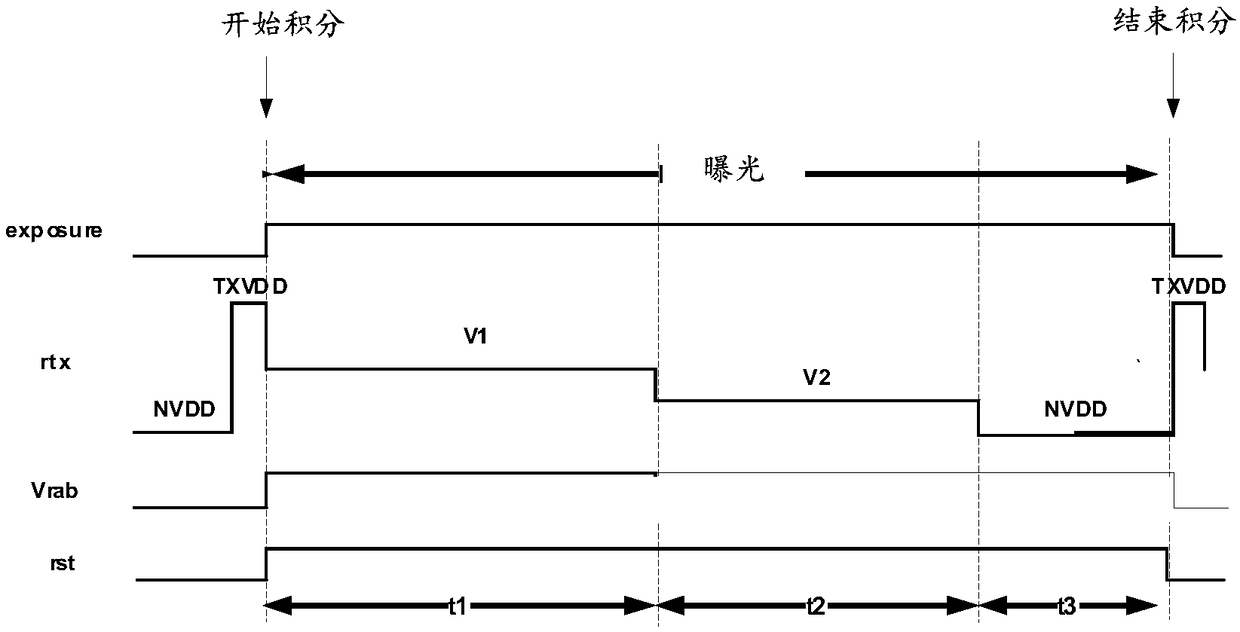
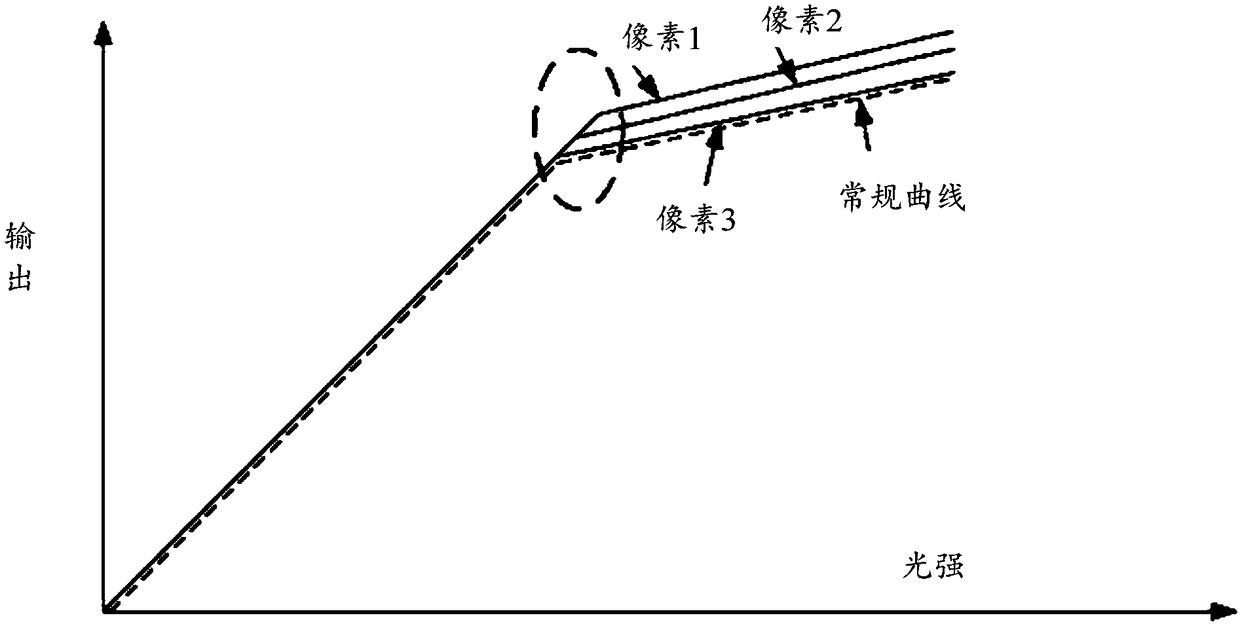
[0062] see figure 1 ,Such as figure 1 As shown, the inflection point-based HDR image sensor pixel structure provided by the embodiment of the present invention includes a photodiode pd for accumulating charges generated by the photoelectric effect in response to incident light, the photodiode has a first terminal and a second terminal, the first terminal connected to the ground terminal, and the second terminal is respectively coupled to the floating diffusion node FD through two branches, one of which is a rolling exposure transfer unit, and the other branch is a global exposure transfer unit; in this embodiment, the rolling exposure The transmission unit is a rolling exposure transmission transistor RTX, and the second terminal of the photodiode pd is coupled to the floating diffusion node FD through the rolling exposure transmission transistor RTX. The global exposure transfer unit includes a global exposure transfer transistor GTX, an exposure control transistor SSG and a...
Embodiment 2
[0111] see Figure 5 ,Such as Figure 5 As shown, compared with Embodiment 1, in the inflection point-based HDR image sensor pixel structure provided by the embodiment of the present invention, the storage capacitor Cm is a parasitic capacitance, specifically, the storage capacitor Cm is the parasitic capacitance of the exposure control transistor SSG to ground. Apart from this, other aspects of this embodiment are the same as those of Embodiment 1, and will not be repeated here.
Embodiment 3
[0113] see Figure 6 ,Such as Figure 6 As shown, this embodiment provides an imaging system 100, including a pixel array 110, the pixel array 110 is arranged in rows and columns, and the structure of each pixel in the pixel array 110 can be the embodiment 1 to embodiment 2 For any one of the pixel structures, please refer to Embodiment 1 to Embodiment 2 for details of the pixel structure, which will not be repeated here.
[0114] In addition, as an exemplary embodiment, the imaging system further includes a logic control unit 120, a drive unit, a column A / D conversion unit 150, and an image processing unit 160; wherein:
[0115] The logic control unit 120 is used to control the working sequence logic of the whole system;
[0116] One end of the drive unit is connected to the logic control unit 120, and the other end is coupled to the pixel array 110 for driving and controlling each control signal line in the pixel array 110; specifically, the drive unit includes a row drive...
PUM
 Abstract
Description
Claims
Application Information


