Image sensor and formation method thereof

A technology for image sensors and pixel areas, applied in radiation control devices, etc., can solve problems such as poor performance of CMOS image sensors, and achieve the effect of improving quantum conversion efficiency and reducing difficulty

Inactive Publication Date: 2018-08-21
HUAIAN IMAGING DEVICE MFGR CORP
View PDF8 Cites 4 Cited by
  • Summary
  • Abstract
  • Description
  • Claims
  • Application Information

AI Technical Summary

Problems solved by technology

[0004] However, the performance of existing CMOS image sensors is still poor

Method used


Image

  • Image sensor and formation method thereof
  • Image sensor and formation method thereof
  • Image sensor and formation method thereof

Examples


Embodiment Construction

[0023] As mentioned in the background, CMOS image sensors have poor performance.

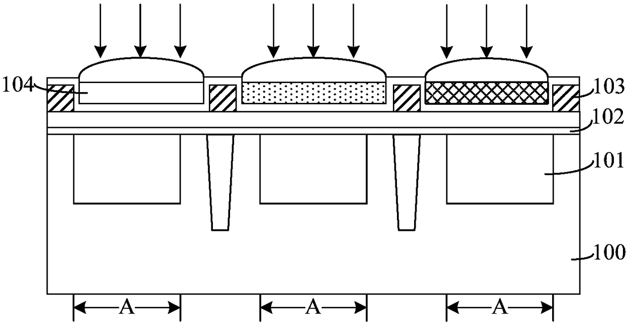
[0024] figure 1 It is a schematic diagram of the structure of a front-illuminated CMOS image sensor.

[0025] Please refer to figure 1 , provide a substrate 100, the substrate 100 includes a number of pixel regions A separated from each other; an isolation layer 102 located on the surface of the substrate 100; a metal grid 103 located on the top of the isolation layer 102 between adjacent pixel regions A, the metal grid The side wall of 103 is perpendicular to the bottom; several color filters 104 at the top of the isolation layer 102 in the pixel region A, the color filters 104 cover the side walls of the metal grid 103; the lens structure at the top of the color filter 104 (not marked in the figure out).

[0026] In the above front-illuminated CMOS image sensor, the metal grid 103 is used to block incident light from entering the adjacent color filter 104 . When the width of the metal grid...


PUM


Abstract

The invention provides an image sensor and a formation method thereof. The formation method comprises the steps that a substrate is provided, the substrate comprises a plurality of pixel areas separate from one another; a block structure is formed on the surface of the substrate between each pair of adjacent pixel areas, the size of the bottom of each block structure is larger than that of the topof the corresponding block structure, and the side wall and bottom of each block structure have an acute angle; a color filter is formed on the surface of the substrate in each pixel area, and the color filters cover the side walls of the block structures. The image sensor formed by using the method has better performance.

Description

technical field [0001] The invention relates to the technical field of semiconductor manufacturing, in particular to an image sensor and a forming method thereof. Background technique [0002] Image sensors are semiconductor devices that convert optical image signals into electrical signals. CMOS (Complementary Metal Oxide Semiconductor) image sensor is a fast-growing solid-state image sensor. Since the image sensor part and the control circuit part of the CMOS image sensor are integrated in the same chip, the CMOS image sensor is small in size and low in power consumption. , low price, compared with the traditional CCD (charge-coupled) image sensor, it has more advantages and is easier to popularize. [0003] Existing CMOS image sensors include photosensors for converting optical signals into electrical signals, and the photosensors are photodiodes formed in a silicon substrate. In addition, a dielectric layer is formed on the surface of the silicon substrate on which the...

Claims


Application Information

Patent Timeline
Patent Type & Authority Applications(China)
IPC IPC(8): H01L27/146
Inventor 周艮梅穆钰平黄晓橹
Owner HUAIAN IMAGING DEVICE MFGR CORP
Why Eureka
Try Eureka