Image sensor and manufacturing method thereof

An image sensor and wafer technology, applied in the field of image sensors, can solve problems such as poor performance of CMOS image sensors, and achieve the effects of improving quantum conversion efficiency, good absorption, and easy application

Active Publication Date: 2019-03-12
OMNIVISION TECH (SHANGHAI) CO LTD
View PDF2 Cites 0 Cited by
  • Summary
  • Abstract
  • Description
  • Claims
  • Application Information

AI Technical Summary

Problems solved by technology

In order to improve the quantum efficiency of infrared light, the overall thickness of the silicon substrate is often increased in the prior art, however, the performance of the CMOS image sensor obtained by this method is not good

Method used


Image

  • Image sensor and manufacturing method thereof
  • Image sensor and manufacturing method thereof
  • Image sensor and manufacturing method thereof

Examples


preparation example Construction

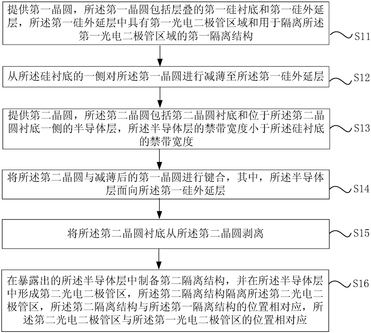
[0038] According to the above research, the present invention provides a method for preparing an image sensor, providing a method for preparing an image sensor, such as figure 1 shown, including the following steps:

[0039] Step S11, providing a first wafer, the first wafer includes a stacked first silicon substrate and a first silicon epitaxial layer, the first silicon epitaxial layer has a first photodiode region and is used to isolate the a first isolation structure for the first photodiode region;

[0040] Step S12, thinning the first wafer to the first silicon epitaxial layer from one side of the silicon substrate;

[0041] Step S13, providing a second wafer, the second wafer includes a second wafer substrate and a semiconductor layer on one side of the second wafer substrate, the semiconductor layer has a band gap smaller than that of the silicon The bandgap width of the substrate;

[0042] Step S14, bonding the second wafer to the thinned first wafer, wherein the se...


PUM


Abstract

The invention discloses an image sensor and a preparation method thereof. The preparation method comprises the following steps: providing a first wafer which includes a first silicon substrate, a first silicon epitaxial layer and an interconnection layer which are successively laminated; thinning the first wafer from one side of the silicon substrate till the first silicon epitaxial layer; providing a second wafer which includes a second wafer substrate and a semiconductor layer which is arranged on one side of the second wafer substrate; bonding the second wafer and the thinned first wafer, the semiconductor layer facing towards the first silicon epitaxial layer; peeling the second wafer substrate from the second wafer; preparing a second isolation structure in the exposed semiconductor layer, and forming a second photoelectric diode region in the semiconductor layer. The semiconductor layer has a forbidden band with a width smaller than that of silicon. The image sensor can better absorb infrared lights, and effectively increase quantum conversion efficiency of a CMOS image sensor.

Description

technical field [0001] The invention relates to the technical field of image sensors, in particular to an image sensor and a preparation method thereof. Background technique [0002] With the rapid development of the mobile Internet, people's demand for smart terminals is increasing, and image sensors, known as the "eyes" of smart terminals, have also ushered in unprecedented development space. The traditional CCD (Charge-coupled Device, charge-coupled device) image sensor is limited in high-performance digital cameras due to its high power consumption; Moreover, it is easy to be compatible with existing semiconductor processes, and the production cost is low, which makes CMOS image sensors occupy half of the image sensor market. [0003] The main problem encountered by CMOS image sensors is the low quantum efficiency (QE, quantum efficiency) of near-infrared light. Quantum efficiency refers to the probability of a photon being transformed into a photogenerated electron in...

Claims


Application Information

Patent Timeline
Patent Type & Authority Patents(China)
IPC IPC(8): H01L27/146
CPCH01L27/14601H01L27/14636H01L27/14643H01L27/14669H01L27/14683H01L27/14685H01L27/1469
Inventor 刘远良肖海波
Owner OMNIVISION TECH (SHANGHAI) CO LTD
Why Eureka
Try Eureka