Manufacturing method of semiconductor element

A manufacturing method and semiconductor technology, applied in the direction of semiconductor/solid-state device manufacturing, semiconductor devices, electrical components, etc., can solve the problems of manufacturing process technology bottlenecks, high costs, etc., and achieve the goal of increasing mobility, reducing parasitic capacitance, and increasing drive current Effect

Active Publication Date: 2021-05-25
POWERCHIP SEMICON MFG CORP
View PDF7 Cites 0 Cited by
  • Summary
  • Abstract
  • Description
  • Claims
  • Application Information

AI Technical Summary

Problems solved by technology

However, since the current technology for reducing the size of components is limited by factors such as manufacturing process technology bottlenecks and high costs, it is necessary to develop other technologies that are different from reducing components to improve the drive current of the components.

Method used


Image

  • Manufacturing method of semiconductor element
  • Manufacturing method of semiconductor element
  • Manufacturing method of semiconductor element

Examples


Embodiment Construction

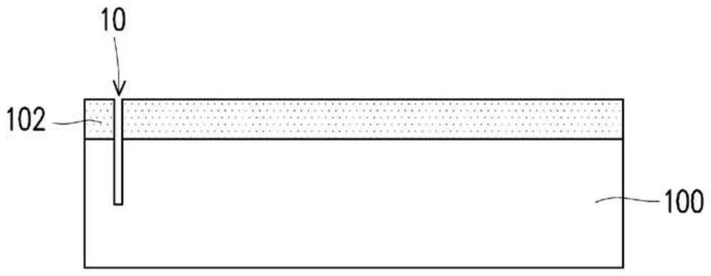
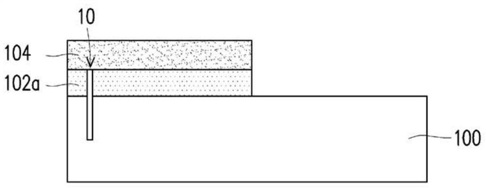
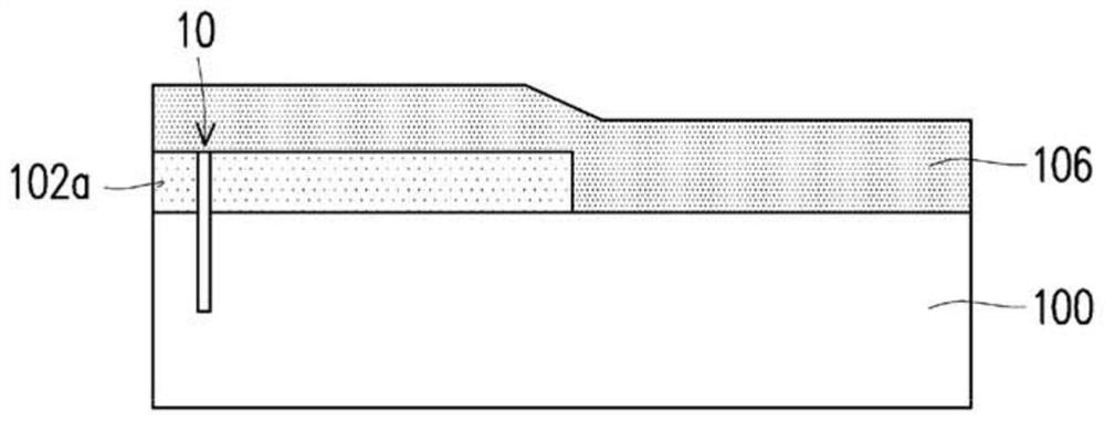
[0056] In the following embodiments, when the first stress layer is a tensile stress layer, the second stress layer is a compressive stress layer; when the first stress layer is a compressive stress layer, the second stress layer is a tensile stress layer. In this embodiment, it is illustrated by taking the first stress layer as a tensile stress layer and the second stress layer as a compressive stress layer as an example, but the present invention is not limited thereto.

[0057] In addition, the thicknesses of layers and regions in the drawings may be exaggerated for clarity. The same or similar reference numbers indicate the same or similar elements, and the following paragraphs will not repeat them one by one.

[0058] In addition, in order to easily describe the relationship between one component or feature and another component or feature depicted in the drawings, for example, "under", "under", "lower part", "under", etc. may be used herein. Spatially relative terms for...


PUM

PropertyMeasurementUnit
thicknessaaaaaaaaaa
tensile stressaaaaaaaaaa
compressive stressaaaaaaaaaa

Abstract

The invention discloses a method for manufacturing a semiconductor element, which includes the following steps. A first stress layer and a second stress layer are respectively formed on the base. A buffer layer is formed on the first stress layer and the second stress layer. Implantation process is performed on the substrate to form a pre-cut surface in the substrate below the first stress layer and the second stress layer. A bonding process is performed to bond the carrier board to the buffer layer. A heat treatment is performed such that a portion of the substrate is separated from the pre-cut facet. The front-end fabrication process is performed on the pre-cut side of another part of the substrate.

Description

technical field [0001] The present invention relates to a manufacturing method of an integrated circuit, and in particular to a manufacturing method of a semiconductor element. Background technique [0002] During the development of semiconductor devices, the size of the device (ie, gate width and channel length) is often reduced to achieve high-speed operation and low power consumption. However, since the current technology for reducing device size is limited by factors such as manufacturing process technology bottlenecks and high costs, it is necessary to develop other technologies different from device reduction to improve the driving current of the device. [0003] Therefore, the industry currently proposes a method of controlling strain to increase device performance, so as to overcome the limit of device miniaturization. The method of controlling the strain refers to forming a stress layer in the semiconductor element, so that the channel region of the element is stra...

Claims


Application Information

Patent Timeline
Patent Type & Authority Patents(China)
IPC IPC(8): H01L21/8238H01L29/78
CPCH01L21/8238H01L29/7842
Inventor 李世平陈昱安黄绣雯张娟华
Owner POWERCHIP SEMICON MFG CORP
Why Eureka
Try Eureka