HDR image sensor pixel structure and imaging system

A technology of image sensor and pixel structure, which is applied in the field of image sensor, can solve the problems such as the difficult realization of requirements, and achieve the effect of preventing halo and high dynamic range characteristics

Active Publication Date: 2018-08-31
思特威(上海)电子科技股份有限公司
View PDF4 Cites 18 Cited by
  • Summary
  • Abstract
  • Description
  • Claims
  • Application Information

AI Technical Summary

Problems solved by technology

[0002] In recent years, the CMOS image sensor industry has developed rapidly, and the chip area of ​​the image sensor has become smaller and smaller. With the reduction of the pixel size, it is necessary for the image sensor to perform in a wide range of lighting conditions (from low light conditions to bright light conditions). requirements become more difficult to achieve

Method used


Image

  • HDR image sensor pixel structure and imaging system
  • HDR image sensor pixel structure and imaging system
  • HDR image sensor pixel structure and imaging system

Examples


Embodiment 1

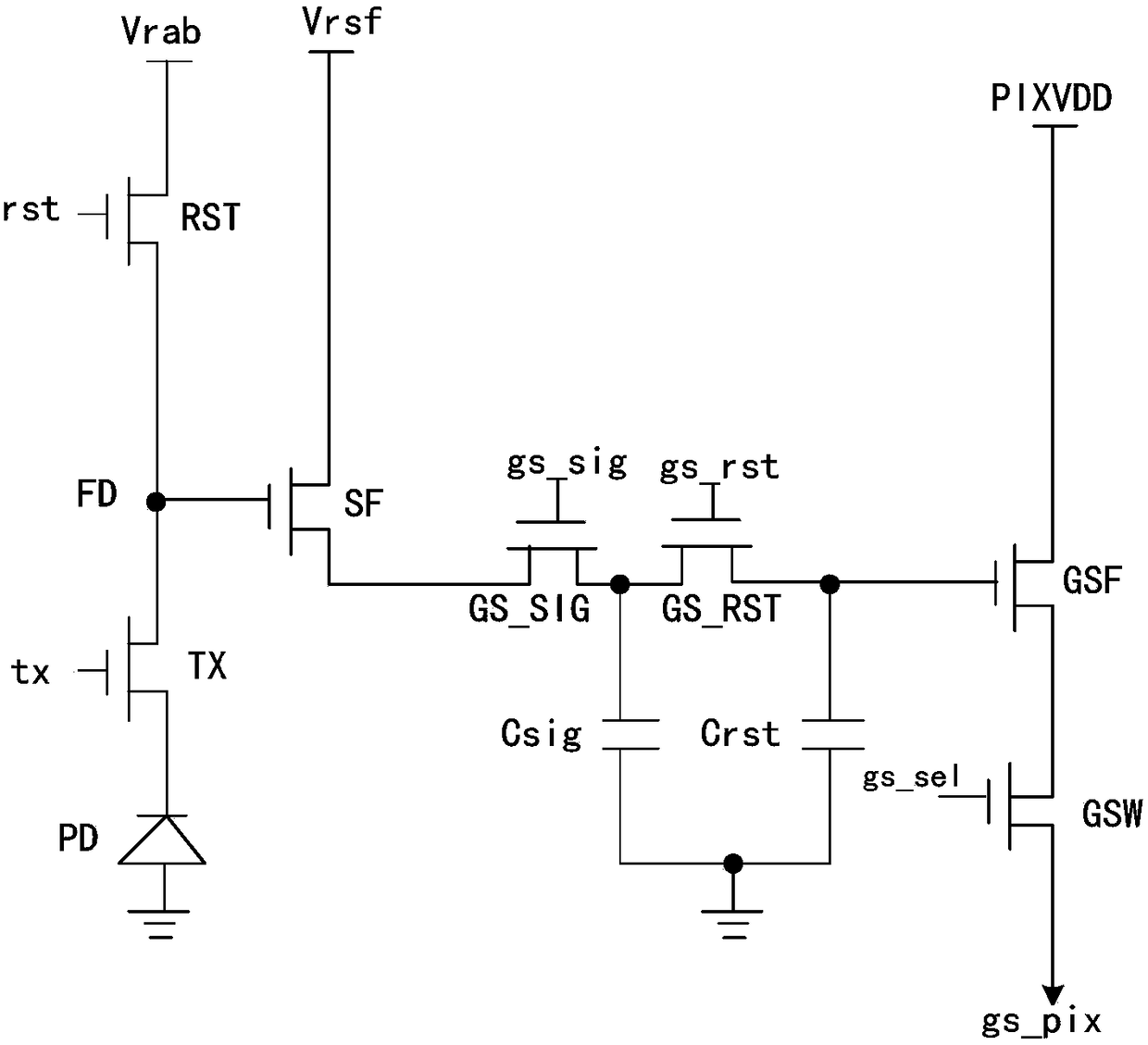
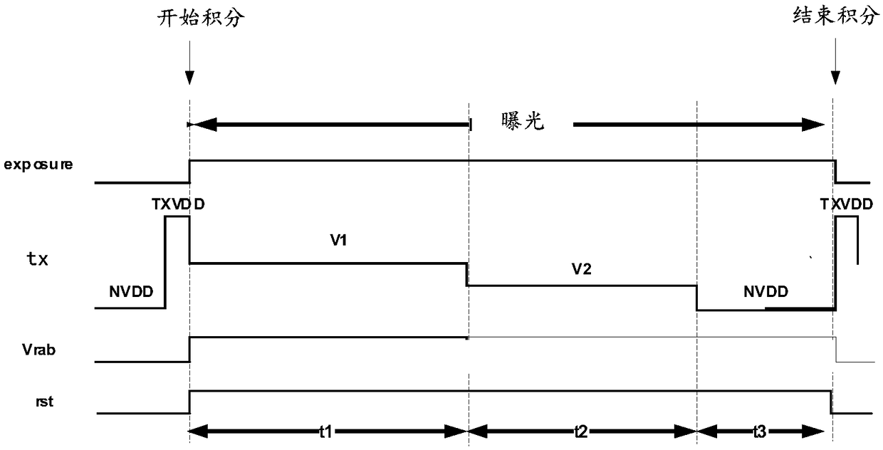
[0082] see figure 1 ,Such as figure 1 As shown, the HDR image sensor pixel structure provided by the embodiment of the present invention includes a photodiode PD, a reset transistor RST, a transfer transistor TX, a first output unit, a signal storage unit and a second output unit. Wherein, the photodiode PD is used for accumulating the charge generated by the photoelectric effect to respond to the incident light. The photodiode PD has a first terminal and a second terminal, the first terminal is connected to the ground terminal, and the second terminal is coupled to the floating terminal through the transfer transistor TX. The diffusion node FD and the transfer transistor TX are used to transfer the charge accumulated in the photodiode PD during the exposure process to the floating diffusion node FD and to provide a balance current to control the full well charge and change the transfer gain during the exposure process of the photodiode PD.

[0083] The reset transistor RST i...

Embodiment 2

[0117] Please refer to Figure 4 ,Such as Figure 4 As shown, in this embodiment, on the basis of Embodiment 1, between the output terminal of the first output unit (denoted as PIXO) and the column output line gs_pix, for example, the source of the first source follower transistor SF and the column output line gs_pix A rolling exposure output transistor RSW is coupled between them. This is because for the circuit structure proposed in Embodiment 1, since the circuit works in the charge domain, the overall power consumption is low, but the first storage capacitor Crst and the second storage capacitor Csig need to be charged and charged during the reading process of the knee voltage. The process of discharging, charging and discharging not only consumes a lot of power consumption, but also requires a longer settling time, which affects the overall reading speed. In this embodiment, by adding a rolling exposure output transistor RSW between the output terminal of the first outp...

Embodiment 3

[0123] Please refer to Figure 6 ,Such as Figure 6 As shown, on the basis of Embodiment 2, this embodiment further adds a dual-conversion gain control unit, which is coupled between the reset transistor RST and the floating diffusion node FD, for realizing gain control and charge storage. As a specific implementation, the dual conversion gain control unit includes a dual conversion gain control transistor DCG and a dual conversion gain capacitor Cdcg, the dual conversion gain control transistor DCG is coupled between the reset transistor RST and the floating diffusion node FD; the dual conversion gain capacitor Cdcg The first terminal of D is coupled to the node between the dual conversion gain transistor DCG and the reset transistor RST, and the second terminal thereof is connected to a specified level. Wherein, the dual conversion gain transistor DCG may be, for example, an NMOS, and its gate receives the control signal dcg.

[0124] In this embodiment, the dual conversio...


PUM


Abstract

The invention discloses an HDR image sensor pixel structure and an imaging system. A reset transistor of the pixel structure is coupled between a floating diffusion node and a first voltage source; aphotodiode is coupled to the floating diffusion node through a transmission unit; and the floating diffusion node is coupled to a column output line through a first output unit, a signal storage unit,and a second output unit in sequence. Because the transmission unit can provide a balancing current during the exposure process of the photodiode to control a full well charge, the signal transmission gain is changed, so that the pixel structure has the high dynamic range characteristic.

Description

technical field [0001] The present invention relates to the technical field of image sensors, in particular to an HDR image sensor pixel structure and an imaging system. Background technique [0002] In recent years, the CMOS image sensor industry has developed rapidly, and the chip area of ​​the image sensor has become smaller and smaller. With the reduction of the pixel size, it is necessary for the image sensor to perform in a wide range of lighting conditions (from low light conditions to bright light conditions). requirements become more difficult to achieve. This performance capability is often referred to as having high dynamic range imaging (HDR). In conventional image capture devices, a pixel unit requires multiple sequential exposures to achieve HDR. Contents of the invention [0003] The object of the present invention is to provide an HDR image sensor pixel structure and an imaging system to realize high dynamic range imaging. [0004] In order to solve the ...

Claims


Application Information

Patent Timeline
Patent Type & Authority Applications(China)
IPC IPC(8): H01L27/146H04N5/374H04N5/3745
CPCH01L27/14643H01L27/14679H04N25/76H04N25/77
Inventor 莫要武徐辰张正民任冠京高哲谢晓邵泽旭马伟剑石文杰
Owner 思特威(上海)电子科技股份有限公司
Why Eureka
Try Eureka