
Surface forming state monitoring device and method for electron beam fuse additive manufacturing

A state monitoring device and additive manufacturing technology, applied in the direction of measuring devices, optical devices, radio wave measurement systems, etc., can solve the problems of poor real-time performance, poor detection effect, and high frequency of signal collection, etc., and achieve fast detection speed and structure Simple, Sensitive Effects

Active Publication Date: 2018-09-04
HUAZHONG UNIV OF SCI & TECH
View PDF13 Cites 2 Cited by
  • Summary
  • Abstract
  • Description
  • Claims
  • Application Information

AI Technical Summary

Problems solved by technology

[0004]1. The plasma light signal obtained by the spectrometer is used to obtain the relevant characteristics of the formed part. This method is difficult to solve the problem that the collection and transmission of the light signal are susceptible to interference and extract the characteristic signal The heavy workload leads to low precision and poor real-time performance;
[0005]2. Measure the surface temperature of the molten pool by a color CCD camera thermometer, and realize the monitoring of the additive manufacturing process through the correlation between the fuse temperature and the quality of the formed part, but The thermal signal of this method is easily interfered by the plasma, resulting in large errors in the detection results;
[0006]3. The method of monitoring the transition form of the fuse through the acoustic signal is poor in the detection effect due to the many and complicated signal collection frequencies and the large processing capacity.
[0007]4. In the process of electron beam fuse additive, factors such as high temperature environment, splash of molten pool, and movement of worktable will make the above monitoring process more difficult

Method used


Image

  • Surface forming state monitoring device and method for electron beam fuse additive manufacturing
  • Surface forming state monitoring device and method for electron beam fuse additive manufacturing
  • Surface forming state monitoring device and method for electron beam fuse additive manufacturing

Examples


Embodiment Construction

[0048] In order to make the object, technical solution and advantages of the present invention clearer, the present invention will be further described in detail below in conjunction with the accompanying drawings and embodiments. It should be understood that the specific embodiments described here are only used to explain the present invention, not to limit the present invention. In addition, the technical features involved in the various embodiments of the present invention described below can be combined with each other as long as they do not constitute a conflict with each other. The present invention will be further described in detail below in combination with specific embodiments.

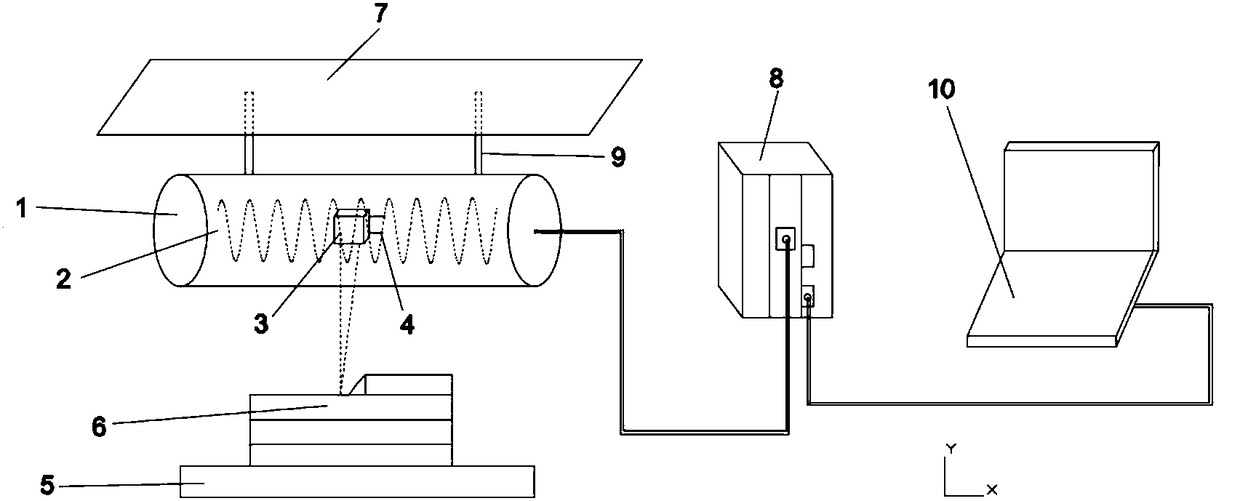
[0049] As a preferred embodiment of the present invention, such as figure 1As shown, the present invention provides a surface forming state monitoring device for electron beam fuse additive manufacturing. Device fixing fixture 9.

[0050] The electromagnetic shielding shell 1 is installed...


PUM


Abstract

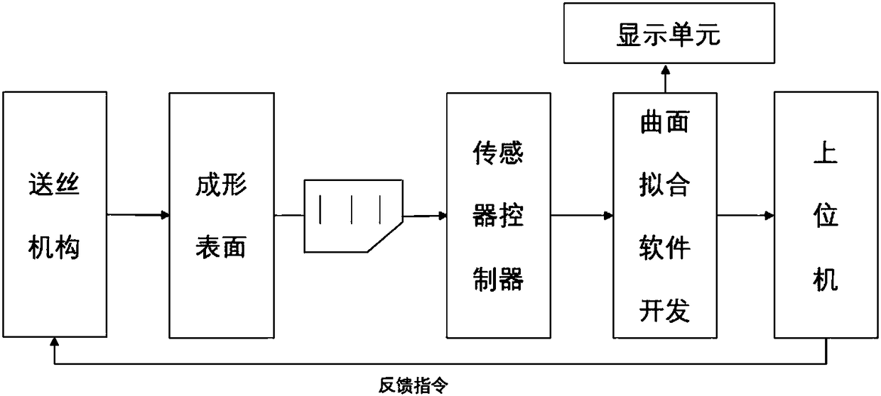
The invention discloses a surface forming state monitoring device for electron beam fuse additive manufacturing. The device comprises an electromagnetic shielding housing, a cooling water pipe, a laser shift sensor, a sensor fixing clamp, a sensor controller and a monitoring device fixing clamp, wherein the electromagnetic shielding housing is mounted on a movement execution mechanism of electronbeam fuse additive manufacturing equipment through the monitoring device fixing clamp; the cooling water pipe is located in the electromagnetic shielding housing; the laser shift sensor is fixed to the cooling water pipe through the sensor fixing clamp, and emits laser to be reflected by a workpiece to receive for ranging; and the sensor controller are separately in transmission connection to thelaser shift sensor and a computer for receiving analog quantity data, including current and voltage, of the laser shift sensor and transmitting the data to the computer, so that the surface forming state of the for electron beam fuse additive materials is precisely monitored in real time.

Description

technical field [0001] The invention belongs to the field of advanced manufacturing technology and precision measurement and control technology, and in particular relates to a surface forming state monitoring device and method for electron beam fuse additive manufacturing. Background technique [0002] Electron beam additive manufacturing refers to using high-energy-density electron beams as heat sources, using computers to process the three-dimensional CAD model of parts in layers, obtaining the two-dimensional profile information of the cross-section of each layer and generating processing paths, according to the predetermined processing path, In the vacuum chamber, the fed wire or powder is melted and piled up layer by layer, finally realizing the near-net shape direct manufacturing of complex metal parts. Electron beam additive manufacturing includes electron beam selective melting and electron beam fuse additive. Due to process differences, electron beam selective melti...

Claims


Application Information

Patent Timeline
IPC IPC(8): G01B11/00G01B11/24G01S17/48G05B13/04
CPCG05B13/042G01B11/002G01B11/24G01S17/48Y02P10/25
Inventor 庞盛永黄康黄安国
Owner HUAZHONG UNIV OF SCI & TECH
Learn More