
Si<3>N<4>/SiON composite film, laser chip and preparation method

A composite film and laser technology, applied in lasers, laser parts, semiconductor lasers, etc., can solve the problem that the passivation film layer cannot meet the performance requirements of high-speed laser chips, and achieve the reduction of stress superposition effect, low film layer stress performance, The effect of meeting performance requirements

Inactive Publication Date: 2018-09-04
HISENSE BROADBAND MULTIMEDIA TECH
View PDF4 Cites 2 Cited by
  • Summary
  • Abstract
  • Description
  • Claims
  • Application Information

AI Technical Summary

Problems solved by technology

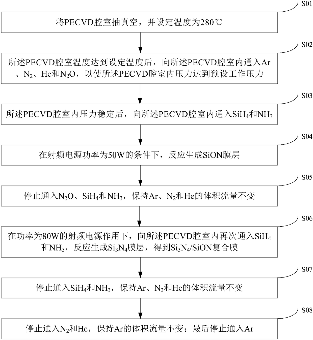
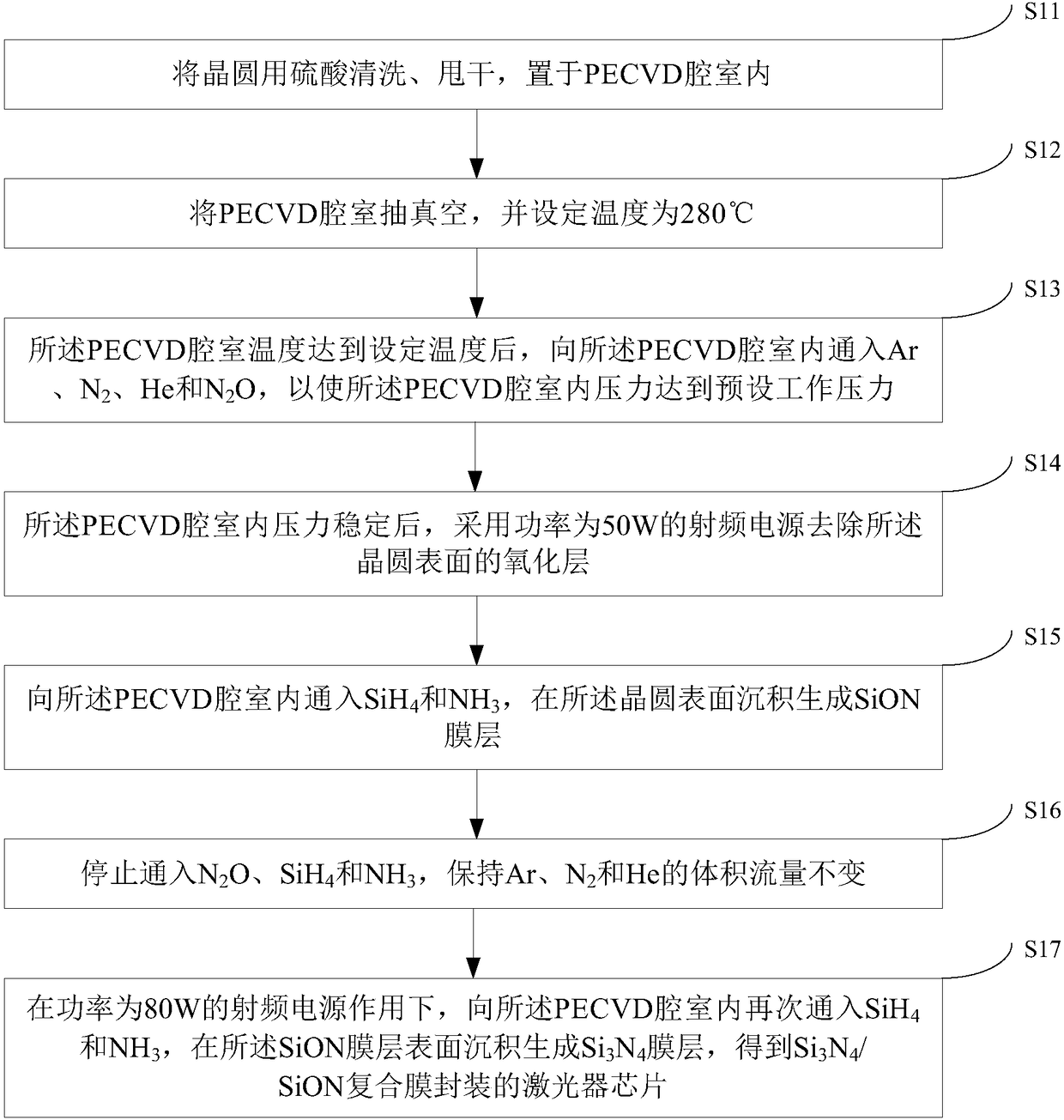
[0005] The invention provides a Si 3 N 4 / SiON composite film, laser chip and preparation method to solve the problem that the currently used passivation film cannot meet the performance requirements of high-speed laser chips

Method used


Image

  • Si&lt;3&gt;N&lt;4&gt;/SiON composite film, laser chip and preparation method
  • Si&lt;3&gt;N&lt;4&gt;/SiON composite film, laser chip and preparation method
  • Si&lt;3&gt;N&lt;4&gt;/SiON composite film, laser chip and preparation method

Examples


Embodiment Construction

[0037]Although PECVD has the advantages of low substrate temperature, good film quality, and fewer pinholes, the passivation film formed by PECVD has a certain film stress, and the greater the thickness of the passivation film, the greater the film stress. Big. When the thickness of the passivation film is relatively thick, the passivation film is easy to crack and fall off, so that the passivation film cannot meet the performance requirements of the laser chip, which in turn leads to failure of the laser chip. However, if the passivation film formed by PECVD is thinner, its water vapor resistance will be poorer, which will cause the laser chip to be easily immersed in water, which will lead to its failure. It can be seen that the water vapor resistance and film stress performance of the passivation film are related to the thickness of the passivation film, and the greater the thickness of the passivation film, the better the water vapor resistance and the greater the film str...


PUM


Abstract

The invention provides a Si<3>N<4> / SiON composite film, a laser chip and a preparation method. The film layer stress of a Si<3>N<4> film layer prepared by a PECVD method is negative stress, while thefilm layer stress of a SiON film layer prepared by the PECVD method is positive stress. By enabling the Si<3>N<4> film layer with negative stress to be compounded with the SiON film layer with positive stress, the Si<3>N<4> / SiON composite film with relatively low stress is formed, thereby lowering a stress overlaying effect in the chip preparation process; and in addition, the Si<3>N<4> film layerand the SiON film layer both have relatively high water vapor resistance performance, so that the prepared Si<3>N<4> / SiON composite film obtains both of water vapor resistance performance and low film stress performance, so that performance requirement of a high-speed laser chip is satisfied.

Description

technical field [0001] The invention relates to the technical field of optical fiber communication, in particular to a Si 3 N 4 / SiON composite film, laser chip and preparation method. Background technique [0002] Semiconductor lasers have the characteristics of small size, light weight and high photoelectric conversion efficiency, so they are widely used in the fields of material processing, medical beauty, military industry and communication. Semiconductor lasers are assembled and packaged to form laser chips to form different integrated circuits. [0003] At present, methods for packaging semiconductor lasers to form laser chips mainly include hermetic packaging and non-hermetic packaging. Non-hermetic packages have lower fabrication costs than hermetic packages. In order to reduce the production cost of laser chips, non-hermetic packaging has been developed rapidly. The more commonly used method for non-hermetic packaging is to form a passivation film layer, that i...

Claims


Application Information

Patent Timeline
IPC IPC(8): H01S5/028
Inventor 逯心红王忠政洪志苍方瑞禹
Owner HISENSE BROADBAND MULTIMEDIA TECH
Learn More