GaAs-base bi-color quantum well infrared detector based on resonance tunneling effect

A technology of infrared detectors and quantum wells, applied in semiconductor devices, sustainable manufacturing/processing, electrical components, etc., can solve the problems of complex device preparation process, difficult material growth, incompatible preparation process, etc., to simplify material growth , reduce dark current, increase the effect of operating temperature

Pending Publication Date: 2018-09-11
SHANGHAI INST OF TECHNICAL PHYSICS - CHINESE ACAD OF SCI
View PDF0 Cites 0 Cited by
  • Summary
  • Abstract
  • Description
  • Claims
  • Application Information

AI Technical Summary

Problems solved by technology

See references Costard, Eric, et al. "Two color QWIP and extended wavebands." Infrared Technology and Applications XXXIII.Vol.6542. International Society for Optics and Photonics, 2007. Compared with traditional single The material growth of the color quantum well detector is more difficult, and the device manufacturing process

Method used


Image

  • GaAs-base bi-color quantum well infrared detector based on resonance tunneling effect
  • GaAs-base bi-color quantum well infrared detector based on resonance tunneling effect
  • GaAs-base bi-color quantum well infrared detector based on resonance tunneling effect

Examples


specific Embodiment 1

[0026] 1.1 Growth of a GaAs-based two-color quantum well material based on resonance tunneling effect with two-color detection peaks at 3 μm and 8 μm:

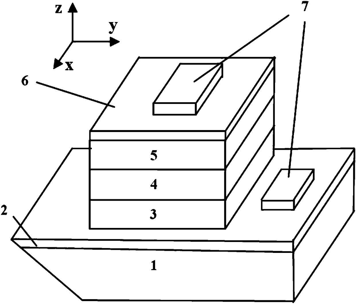
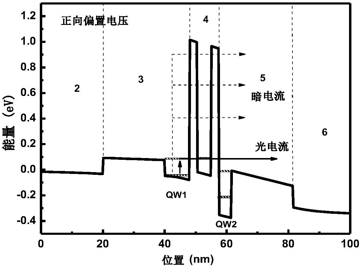
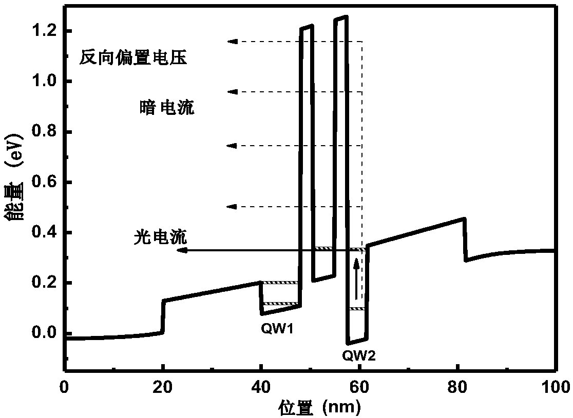
[0027] Using molecular beam epitaxy (MBE) to grow a buffer layer GaAs on the GaAs substrate (1), and then grow the lower electrode layer (2) GaAs:Si, the doped Si concentration is 10 17 / cm 3 , with a thickness of 0.6 μm, and the first quantum well region (3) continues to grow on the lower electrode layer (2), the structure is: barrier Al 0.27 Ga 0.73 As thickness is 40nm, potential well QW 1 The thickness is 5.2nm; QW 1 For GaAs: Si, the doping concentration is 10 17 / cm 3 . Re-grow the resonant tunneling region (4), the growth sequence of this part is: first grow a layer of AlAs barrier layer with a thickness of 2nm, and then grow a layer of 3nm tunneling potential well Al 0.25 Ga 0.75 As, finally grow a 2nm AlAs barrier layer. Continue to grow the second quantum well region (5) after the resonance tunneling region ...

specific Embodiment 2

[0031] 1.1 Growth of a GaAs-based two-color quantum well material based on resonance tunneling effect with two-color detection peaks at 5 μm and 15 μm:

[0032] Using molecular beam epitaxy (MBE) to grow a buffer layer GaAs on the GaAs substrate (1), and then grow the lower electrode layer (2) GaAs: Si, the concentration of doped Si is 5×10 17 cm -3 , with a thickness of 0.6 μm, and the first quantum well region (3) continues to grow on the lower electrode layer (2), the structure is: barrier Al 0.12 Ga 0.88 As thickness is 70nm, potential well QW 1 The thickness is 8nm; QW 1 For GaAs:Si, the doping concentration is 4×10 17 cm -3 . Re-grow the resonant tunneling region (4), the growth sequence of this part is: first grow a layer of AlAs barrier layer with a thickness of 4nm, and then grow a layer of 6nm tunneling potential well Al 0.05 Ga 0.95 As, finally grow a 4nm AlAs barrier layer. Continue to grow the second quantum well region (5) after the resonance tunneling r...

specific Embodiment 3

[0036] 1.1 Growth of a GaAs-based two-color quantum well material based on resonance tunneling effect with two-color detection peaks at 4 μm and 10.5 μm:

[0037] Using molecular beam epitaxy (MBE) to grow a buffer layer GaAs on the GaAs substrate (1), and then grow the lower electrode layer (2) GaAs:Si, the doped Si concentration is 1×10 18 cm -3 , with a thickness of 0.6 μm, and the first quantum well region (3) continues to grow on the lower electrode layer (2), the structure is: barrier Al 0.17 Ga 0.83 As thickness is 55nm, potential well QW 1 Thickness is 6nm; QW 1 For GaAs:Si, the doping concentration is 8×10 17 cm -3 . Re-grow the resonant tunneling region (4), the growth sequence of this part is: first grow a layer of AlAs barrier layer with a thickness of 3nm, and then grow a layer of 4.5nm tunneling potential well Al 0.15 Ga 0.85 As, finally grow a 3nm AlAs barrier layer. Continue to grow the second quantum well region (5) after the resonance tunneling regio...


PUM

PropertyMeasurementUnit
Thicknessaaaaaaaaaa
Thicknessaaaaaaaaaa
Thicknessaaaaaaaaaa

Abstract

The invention discloses a GaAs-base bi-color quantum well infrared detector based on a resonance tunneling effect. The detector is prepared by sequentially growing a lower electrode layer, an active region layer and an upper electrode layer on a GaAs substrate by virtue of a molecular beam epitaxy measure, wherein the active region layer is formed by clamping a resonance tunneling diode structurebetween two different quantum wells. When a specific positive or negative bias is applied to the detector, two waveband light currents produced through the response of quantum wells with different widths selectively run through a resonance tunneling diode so as to form a response loop. Compared with current traditional bi-color quantum well detectors, the GaAs-base bi-color quantum well infrared detector has the advantages that the bi-color detection can be realized through adjusting the direction and size of the applied bias, and the working temperature of the device can be increased; and besides, the preparation process of the detector is relatively simple, and the detector has the important signature to the development of bi-color infrared quantum well detectors.

Description

technical field [0001] The invention relates to a GaAs-based quantum well infrared detector, in particular to a GaAs-based two-color quantum well infrared detector based on the resonance tunneling effect. Background technique [0002] Quantum well infrared detectors are an important part of infrared focal plane thermal imaging systems, especially GaAs-based quantum well infrared detectors, because of their mature material growth and process preparation, easy integration of large area arrays, and good uniformity and stability. Research hotspots in the field of infrared detectors. However, with the continuous development of semiconductor technology, monochromatic infrared detectors can no longer meet the needs of higher integration and more functions, so the development of dual-band or even multi-band window detectors has emerged as the times require. Compared with single-band thermal imaging systems, thermal imaging systems based on dual-color quantum well detectors can dete...

Claims


Application Information

Patent Timeline
IPC IPC(8): H01L31/0352H01L31/109H01L31/18
CPCH01L31/035209H01L31/109H01L31/1844Y02P70/50
Inventor 李宁郑元辽陈平平李志锋杨贺鸣周玉伟唐舟陈效双陆卫
Owner SHANGHAI INST OF TECHNICAL PHYSICS - CHINESE ACAD OF SCI
Why Eureka
Try Eureka