Mechanical arm and semiconductor device

A robotic arm and connecting arm technology, applied in semiconductor/solid state device manufacturing, conveyor objects, electrical components, etc., can solve problems such as wafer offset, robotic arm vibration, wafer collision with production machines, Accurate position and the effect of improving product yield

Inactive Publication Date: 2018-09-14
HUAIAN IMAGING DEVICE MFGR CORP
View PDF3 Cites 5 Cited by
  • Summary
  • Abstract
  • Description
  • Claims
  • Application Information

AI Technical Summary

Problems solved by technology

[0004] However, in the prior art, it is easy for the wafer to be shifted on the robot arm, etc., resulting in the wrong placement of the wafer in the subsequent process, which in turn causes serious process problems
In more serious cases, the wafers carried by the robotic arm may even fail to enter the machine, and the robotic arm may be deflected or bumped, causing the machine to alarm and shut down, etc.
Specifically, after the wafer is shifted on the robot arm, the robot arm still moves according to the original route, which may cause the wafer to collide with the production machine, causing the robot arm to vibrate, and in severe cases, the robot arm may be deflected or bumped

Method used


Image

  • Mechanical arm and semiconductor device
  • Mechanical arm and semiconductor device
  • Mechanical arm and semiconductor device

Examples


Embodiment Construction

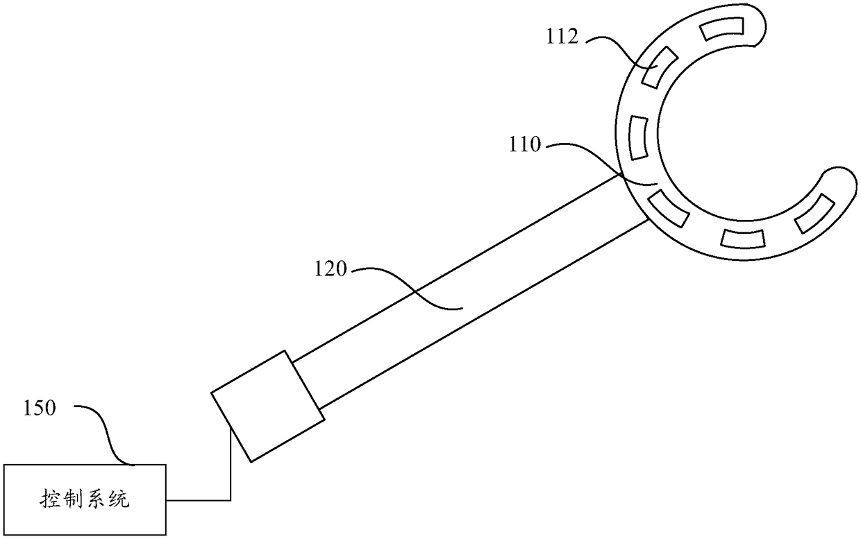
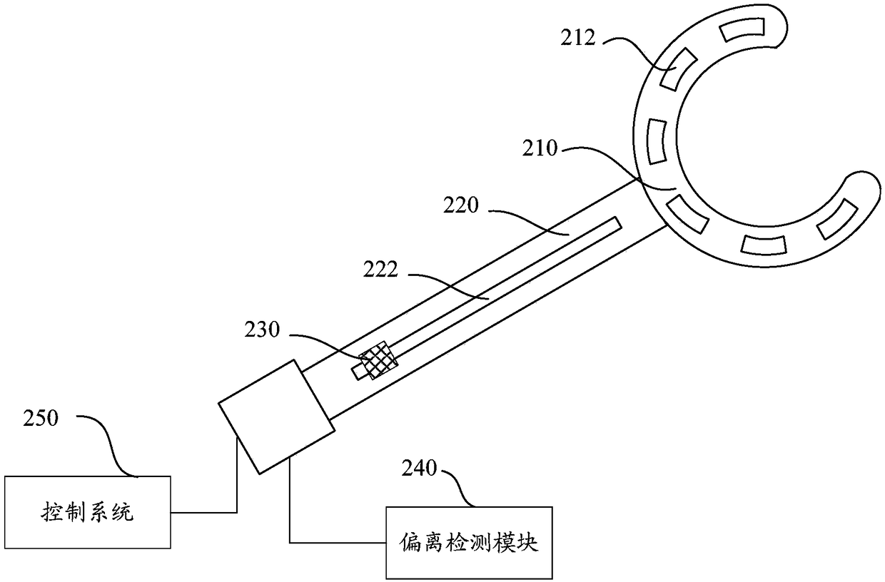
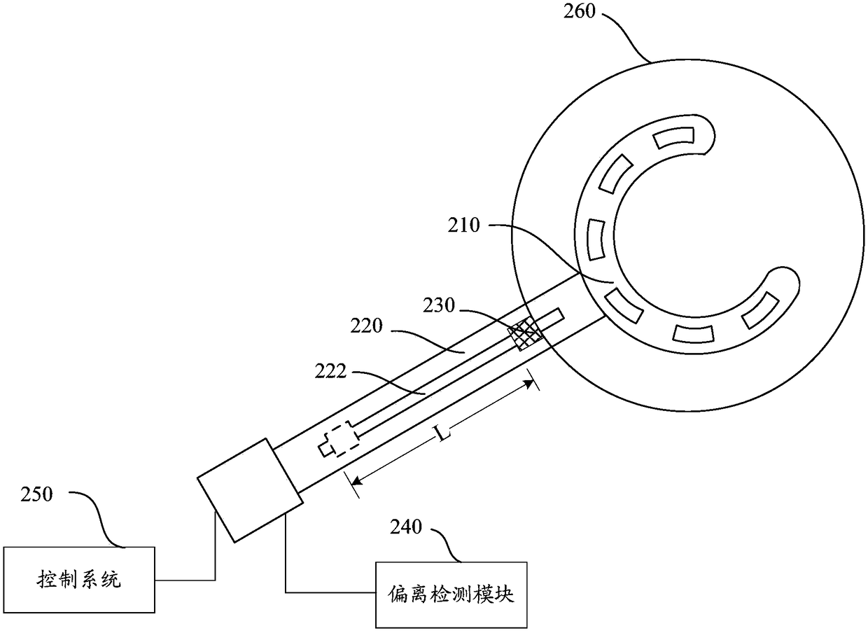
[0030] In the existing robotic arm equipment, the process of using the robotic arm to transfer the wafer usually includes: using the robotic arm to vacuum the wafer from the bottom of the wafer, and then controlling the movement of the robotic arm to carry out send. However, in the prior art, it is easy for the wafer to be shifted on the robot arm, etc., resulting in a wrong placement position of the wafer in the subsequent process, causing serious process problems, and even causing the robot arm to carry Wafers cannot enter the machine, and the robotic arm is deflected or bumped, causing the machine to alarm and stop. Specifically, after the wafer is shifted on the robot arm, the robot arm still moves according to the original route, which may cause the wafer to collide with the production machine, causing the robot arm to vibrate, and in severe cases, the robot arm may be deflected or bumped .

[0031] refer to figure 1 , figure 1 It is a structural schematic diagram of ...


PUM


Abstract

The invention discloses a mechanical arm and a semiconductor device. The mechanical arm comprises an adsorption part, a connection arm, a sliding part and a deviation detection module, wherein the adsorption part is used for absorbing a wafer; the connection arm is connected with the adsorption part, the connection arm is provided with a sliding guide rail, and the extending direction of the sliding guide rail is consistent with that of the connection arm; the sliding part starts sliding from a preset triggering point of the sliding guide rail to abut against the edge of the wafer; and the deviation detection module is used for at least determining the deviation state of the wafer according to the sliding distance of the sliding part. The scheme of the invention can effectively judge the deviation state of the wafer, a deviation condition happening when a wafer is placed in a subsequent process can be avoided, the product yield is thus improved, and the downtime times are reduced.

Description

technical field [0001] The invention relates to the field of semiconductor manufacturing equipment, in particular to a mechanical arm and semiconductor equipment. Background technique [0002] In semiconductor manufacturing equipment, the robotic arm (Arm) is an important part of the machine and plays an important role. Specifically, the robotic arm is used to grab and transfer the wafer (Wafer) in the machine, so as to realize the connection between various modules in the machine, so as to realize the automation function in a machine. [0003] In the existing robotic arm equipment, the process of using the robotic arm to transfer the wafer usually includes: using the robotic arm to vacuum the wafer from the bottom of the wafer, and then controlling the movement of the robotic arm to carry out send. [0004] However, in the prior art, it is easy for the wafer to be shifted on the robot arm, etc., resulting in a wrong placement position of the wafer in the subsequent proces...

Claims


Application Information

Patent Timeline
Patent Type & Authority Applications(China)
IPC IPC(8): H01L21/677H01L21/683H01L21/68
CPCH01L21/67706H01L21/68H01L21/6838
Inventor 张党柱郭甜赖政聪古哲安
Owner HUAIAN IMAGING DEVICE MFGR CORP
Why Eureka
Try Eureka