

Conductive thin film and method for improving conductivity of conductive thin film
A conductive thin film and conductive technology, which is applied in the direction of equipment for manufacturing conductive/semiconductive layers, conductive layers on insulating carriers, circuits, etc., can solve the problems of increasing microwave time, thermal deformation of flexible substrates, and inability of resistance nodes Welding or complete welding and other problems to achieve the effect of reducing sheet resistance
Inactive Publication Date: 2018-09-18
FOSHAN SHUNDE SUN YAT SEN UNIV RES INST +2
View PDF3 Cites 4 Cited by
- Summary
- Abstract
- Description
- Claims
- Application Information
AI Technical Summary
Problems solved by technology
[0002] The traditional transparent conductive thin film material is mainly indium tin oxide (I TO), but because of its poor flexibility, high cost and harsh preparation conditions, and the increasingly scarce metal indium (In) required for the preparation of I TO, it has been Unable to meet the requirements of new electronic devices, a transparent conductive film made of metal nanowires has appeared, which has the most excellent photoelectric properties and excellent mechanical stability. It is considered to be the next generation of ITO. transparent conductive film
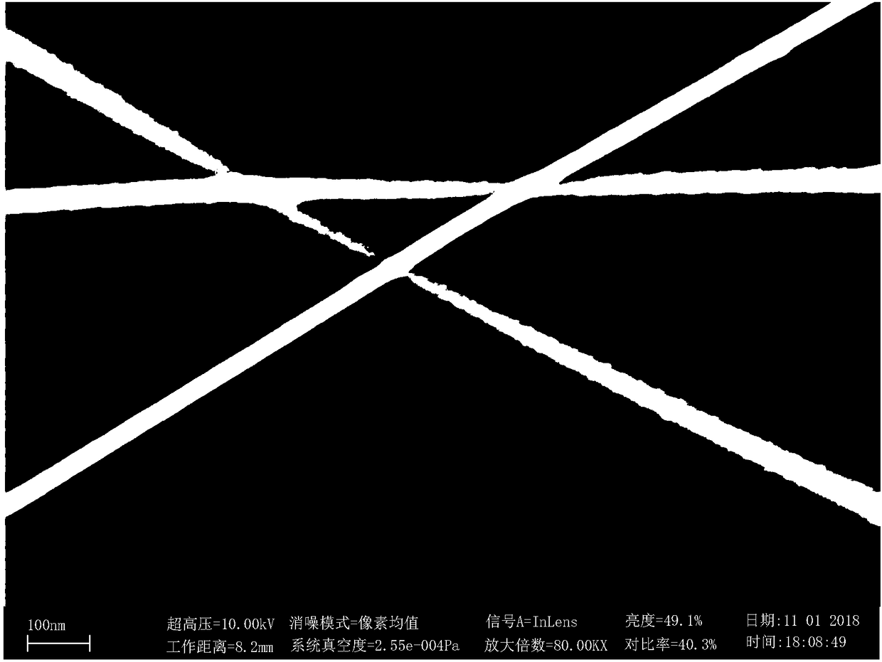
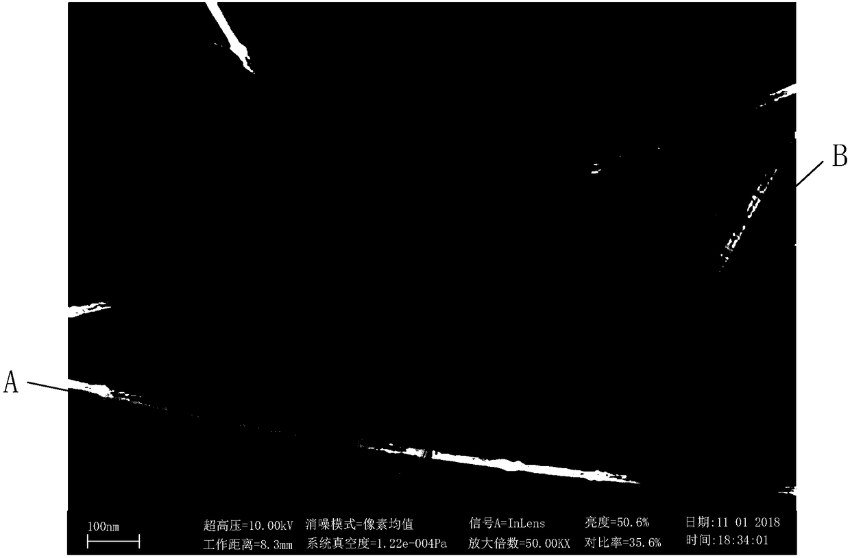
[0003] The silver nanowire conductive film is not a continuous conductor, but a conductive network formed by the conductive path formed by the overlap between the wire and the wire. The contact area between the wire and the wire is very small and the overlap is not firm, which will reduce the The conductivity of the metal nanowire film, how to effectively connect the metal nanowires together has become a problem to be solved. Patent CN104766675A proposes the use of microwaves to process metal nanowires on glass substrates, which can be applied to large-area and efficient welding of nanowires. However, microwave treatment of metal nanowires on flexible substrates has obvious shortcomings, because microwaves are selective and will preferentially weld nodes with high junction resistance. To weld nodes with small junction resistance, it is necessary to Increase the microwave time, and if the microwave time is too long, the junction with high junction resistance will generate more heat, which will easily lead to thermal deformation of the flexible substrate. In order to ensure that the film does not deform, it is necessary to control the microwave time and microwave power, resulting in a large number of Junctions with low resistance are not welded or welded completely
Method used
View moreImage
Smart ImageViewing Examples

Examples
Embodiment 2
[0043] Embodiment 2 is only carrying out composite treatment with metal oxide sol to conductive film;
Embodiment 3
[0044] Embodiment 3 is to carry out composite treatment with metal oxide sol first to conductive film, and then carry out microwave treatment;
Embodiment 4
[0045] Embodiment 4 is to first carry out microwave treatment to the conductive film, and then carry out composite treatment with metal oxide sol;
[0046] The metal nanowire 1 selected in Embodiment 1 to Embodiment 4 is silver nanowire, the flexible substrate material selected is PET material, and the metal oxide sol 2 selected is zinc oxide sol. The specific implementation process is as follows
Login to View More PUM
| Property | Measurement | Unit |
|---|---|---|
| diameter | aaaaa | aaaaa |
Abstract
The invention discloses a conductive thin film, which is characterized in that junction points of a metal nanowire grid are coated by using a metal oxide sol, so that connection between metal nanowires is more closely, and sheet resistance of the conductive thin film is reduced. The method further discloses a method for improving conductivity of the conductive thin film. The method comprises the steps of: firstly, processing the conductive thin film by utilizing microwaves, so that the junction points with large junction resistance among the metal nanowires are welded, thereby reducing the sheet resistance of the conductive thin film; and secondly, painting the metal oxide sol on the conductive thin film after microwave processing, so that unwelded parts of the metal nanowires are in moreclose lap joint by means of the adhesive attraction between the metal oxide and a substrate when the conductive thin film is annealed. In addition, the metal oxide can serve as an electron transport layer of the conductive thin film, the parts with large junction resistance can transport electrons by means of an oxide semiconductor layer, so as to reduce the sheet resistance of the conductive thinfilm, and the sheet resistance of the conductive thin film is reduced through the two-step processing, thereby improving the conductivity of the conductive thin film.
Description
technical field [0001] The invention relates to the field of preparation of transparent conductive films, in particular to a conductive film and a method for improving the conductivity of the conductive film. Background technique [0002] The traditional transparent conductive thin film material is mainly indium tin oxide (I TO), but because of its poor flexibility, high cost and harsh preparation conditions, and the increasingly scarce metal indium (In) required for the preparation of I TO, it has been Unable to meet the requirements of new electronic devices, a transparent conductive film made of metal nanowires has appeared, which has the most excellent photoelectric properties and excellent mechanical stability. It is considered to be the next generation of ITO. Transparent conductive film. [0003] The silver nanowire conductive film is not a continuous conductor, but a conductive network formed by the conductive path formed by the overlap between the wire and the wire...
Claims
Login to View More Application Information
Patent Timeline
 Patent Type & AuthorityApplications(China)
IPC IPC(8): H01B5/14H01B13/00
CPCH01B5/14H01B13/0026
Inventor杨柏儒翁明许钰旺陈鹏张伟李京周王毓成邱景燊柳成林
OwnerFOSHAN SHUNDE SUN YAT SEN UNIV RES INST