Optical detector and preparation method therefor, fingerprint recognition sensor, and display device

An optical detector and fingerprint recognition technology, applied in the fields of fingerprint recognition sensors, optical detectors and their preparation, and display devices, can solve the problem of reduced photosensitive area area, optical detector sensitivity that cannot meet requirements, photodiodes and TFT switches. Large area and other problems, to achieve the effect of reducing the size, increasing the area of ​​the photosensitive area, and improving the sensitivity

Active Publication Date: 2018-09-25
BOE TECH GRP CO LTD
View PDF7 Cites 4 Cited by
  • Summary
  • Abstract
  • Description
  • Claims
  • Application Information

AI Technical Summary

Problems solved by technology

In the actual application of existing optical detectors, it is found that photodiodes and TFT switches often occupy a large area, which reduces the area of ​​the photosensitive area, so that the sensitivity of the optical detector cannot meet the requirements

Method used


Image

  • Optical detector and preparation method therefor, fingerprint recognition sensor, and display device
  • Optical detector and preparation method therefor, fingerprint recognition sensor, and display device
  • Optical detector and preparation method therefor, fingerprint recognition sensor, and display device

Examples


Embodiment 1

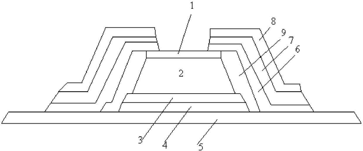
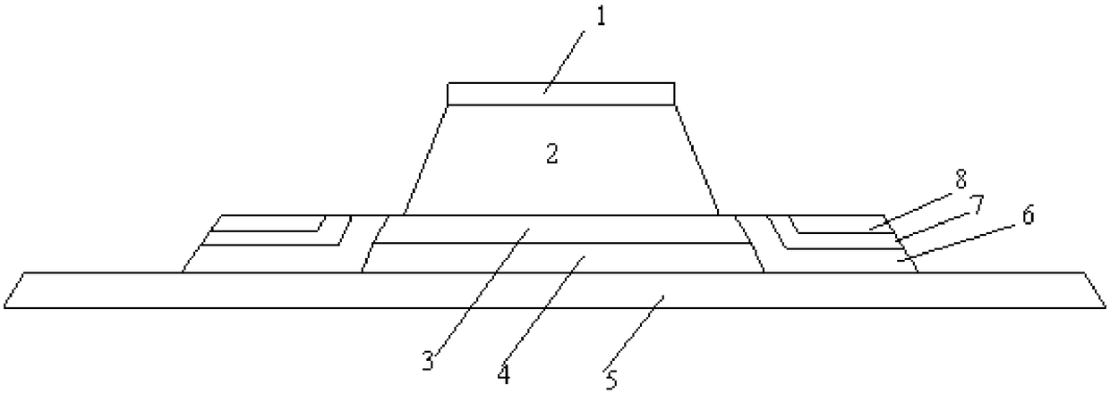
[0040] Figure 1a Schematic diagram of the structure of the optical detector provided in Embodiment 1 of the present invention; Figure 1b for Figure 1a Block diagram of the optical detector shown; see Figure 1a with Figure 1b , the optical detector provided by Embodiment 1 of the present invention includes: a stacked structure of a first electrode 1, a photoelectric conversion layer 2, a second electrode 3, a first insulating layer 4, and a third electrode 5 that are sequentially stacked; the optical detector It also includes an active layer 6 , a gate insulating layer 7 and a gate 8 .

[0041] Wherein, the first electrode 1 and the second electrode 3 are used as the two working electrodes of the photoelectric conversion layer 2, and the first electrode 1 is used as the light-incident electrode. The so-called light-incidence electrode refers to the electrode on which the light signal is incident. A transparent electrode that allows light signals to enter. That is, the fi...

Embodiment 2

[0048] figure 2 The structural representation of the optical detector provided for embodiment 2 of the present invention; Please refer to figure 2 The optical detector provided by Embodiment 2 of the present invention is similar to the optical detector provided by Embodiment 1, and also includes a first electrode 1, a photoelectric conversion layer 2, a second electrode 3, a first insulating layer 4, and a third electrode 5 , the active layer 6 , the gate insulating layer 7 and the gate 8 , since their respective positional relationships and functions have been described in detail in the above-mentioned embodiment 1, they will not be repeated here.

[0049]Only the differences between this embodiment and the above-mentioned Embodiment 1 will be described below. In this embodiment, the second electrode 3 and the third electrode 5 serve as one and the other of the source and the drain, respectively. Specifically, such as figure 2 As shown, the active layer 6 is electricall...

Embodiment 3

[0052] image 3 It is a flow chart of the preparation method of the optical detector provided in Example 3 of the present invention. see image 3 , the preparation method of the optical detector provided by the present embodiment comprises the following steps:

[0053] S1, preparing a first electrode, a photoelectric conversion layer, a second electrode, a first insulating layer, and a third electrode that are sequentially stacked on the substrate.

[0054] S2, preparing an active layer, the active layer is electrically connected to the first electrode and the third electrode, and is insulated from the photoelectric conversion layer and the second electrode;

[0055] S3, preparing a gate insulating layer on the active layer.

[0056] S4, preparing a gate on the gate insulating layer.

[0057] The above step S1 specifically includes but is not limited to:

[0058] Form a third electrode material layer, a first insulating layer material layer, a second electrode material la...


PUM


Abstract

The invention provides an optical detector, and the optical detector comprises a stacked structure where a first electrode, a photoelectric conversion layer, a second electrode, a first insulating layer and a third electrode are sequentially stacked. The optical detector also comprises an active layer, a gate insulating layer and a gate electrode. The first electrode or the second electrode servesas one of a source electrode and a drain electrode. The third electrode serves as the other one of the source electrode and the drain electrode. The gate insulating layer is disposed on the active layer. The gate electrode is disposed on the gate insulating layer. The invention also provides a preparation method for the optical detector, a fingerprint recognition sensor, and a display device. Thelight sensing area of the optical detector can be increased, thereby improving the sensitivity of the optical detector.

Description

technical field [0001] The invention belongs to the field of display technology, and in particular relates to an optical detector and a preparation method thereof, a fingerprint identification sensor and a display device. Background technique [0002] At present, optical detectors such as X-ray detectors and sensors for fingerprint identification have high requirements for detection sensitivity, especially, optical detectors integrated in TFT-LCD displays, and more especially, integrated in high PPI Optical fingerprint detector for TFT-LCD display. The detection sensitivity of the optical detector is relatively high, which requires a large photosensitive area, or in other words, the array where it is located has a large aperture ratio. [0003] The optical detector usually includes a TFT switch and a photoelectric conversion unit (for example, a photodiode), and the source of the TFT switch is connected to the anode of the photodiode. In practical applications of existing ...

Claims


Application Information

Patent Timeline
Patent Type & Authority Applications(China)
IPC IPC(8): H01L27/144H01L21/82G06K9/00
CPCH01L21/82H01L27/1443G06V40/13H01L27/146H01L31/112G06V40/1318H04N23/55H01L21/44G02B6/132G02F1/1343H01L27/1255
Inventor 孙建明宁策张文林
Owner BOE TECH GRP CO LTD
Why Eureka
Try Eureka