Optical detector and preparation method thereof, fingerprint recognition sensor, display device
An optical detector and photoelectric conversion layer technology, applied in the fields of fingerprint identification sensors, display devices, optical detectors and their preparation, can solve the problem of reducing the area of the photosensitive area, the sensitivity of the optical detector cannot meet the requirements, photodiode and TFT switches The problem of large occupied area, etc., can reduce the size, increase the area of the photosensitive area, and improve the sensitivity.
- Summary
- Abstract
- Description
- Claims
- Application Information
AI Technical Summary
Problems solved by technology
Method used
Image
Examples
Embodiment 1
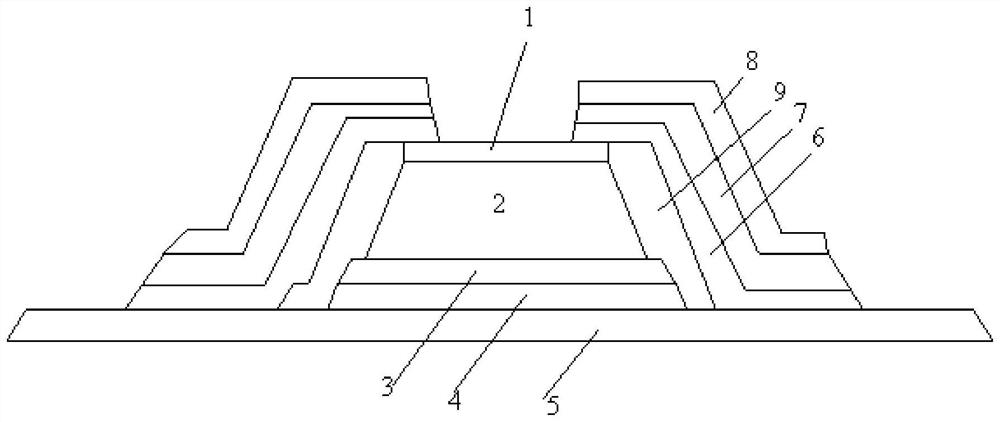
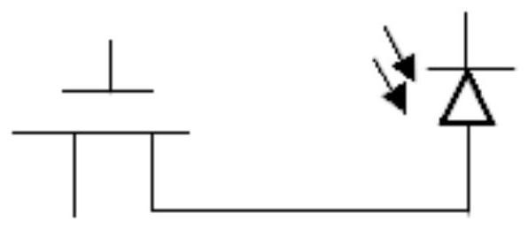
[0040] Figure 1a Schematic diagram of the structure of the optical detector provided in Embodiment 1 of the present invention; Figure 1b for Figure 1a Block diagram of the optical detector shown; see Figure 1a and Figure 1b , the optical detector provided by Embodiment 1 of the present invention includes: a stacked structure of a first electrode 1, a photoelectric conversion layer 2, a second electrode 3, a first insulating layer 4, and a third electrode 5 that are sequentially stacked; the optical detector It also includes an active layer 6 , a gate insulating layer 7 and a gate 8 .
[0041] Wherein, the first electrode 1 and the second electrode 3 are used as the two working electrodes of the photoelectric conversion layer 2, and the first electrode 1 is used as the light-incident electrode. The so-called light-incidence electrode refers to the electrode on which the light signal is incident. A transparent electrode that allows light signals to enter. That is, the fir...
Embodiment 2
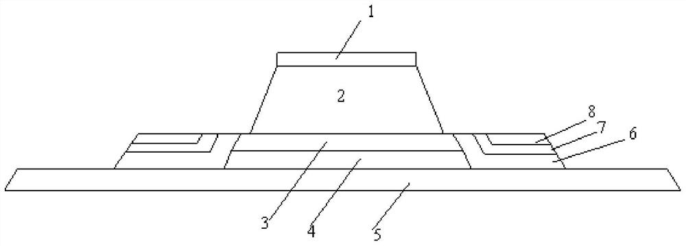
[0048] figure 2 The structural representation of the optical detector provided for embodiment 2 of the present invention; Please refer to figure 2 The optical detector provided by Embodiment 2 of the present invention is similar to the optical detector provided by Embodiment 1, and also includes a first electrode 1, a photoelectric conversion layer 2, a second electrode 3, a first insulating layer 4, and a third electrode 5 , the active layer 6 , the gate insulating layer 7 and the gate 8 , since their respective positional relationships and functions have been described in detail in the above-mentioned embodiment 1, they will not be repeated here.
[0049]Only the differences between this embodiment and the above-mentioned Embodiment 1 will be described below. In this embodiment, the second electrode 3 and the third electrode 5 serve as one and the other of the source and the drain, respectively. Specifically, such as figure 2 As shown, the active layer 6 is electricall...
Embodiment 3
[0052] image 3 It is a flow chart of the preparation method of the optical detector provided in Example 3 of the present invention. see image 3 , the preparation method of the optical detector provided by the present embodiment comprises the following steps:
[0053] S1, preparing a first electrode, a photoelectric conversion layer, a second electrode, a first insulating layer, and a third electrode that are sequentially stacked on the substrate.
[0054] S2, preparing an active layer, the active layer is electrically connected to the first electrode and the third electrode, and is insulated from the photoelectric conversion layer and the second electrode;
[0055] S3, preparing a gate insulating layer on the active layer.
[0056] S4, preparing a gate on the gate insulating layer.
[0057] The above step S1 specifically includes but is not limited to:
[0058] Form a third electrode material layer, a first insulating layer material layer, a second electrode material la...
PUM
 Abstract
Description
Claims
Application Information


