Semiconductor light emitting device

A technology of light-emitting elements and semiconductors, applied in semiconductor devices, electrical components, electric solid-state devices, etc., can solve the problems that the active layer 400 cannot be used for the light-emitting area, and the light-emitting area is reduced, so as to improve the luminous efficiency and prevent the reduction of the light-emitting area. Small, the effect of improving the antistatic characteristics

Inactive Publication Date: 2018-09-25
SEOUL VIOSYS CO LTD
View PDF5 Cites 1 Cited by
  • Summary
  • Abstract
  • Description
  • Claims
  • Application Information

AI Technical Summary

Problems solved by technology

Although the V-pit α has the advantage of being able to improve the antistatic property and improve the reliability of the semiconductor light-emitting element, refer to figure 1 , since the active layer 400 in the region where the V-pit α is formed cannot be used as a light emitting region based on the combination of electrons and holes, there is a problem that the light emitting region decreases accordingly

Method used


Image

  • Semiconductor light emitting device
  • Semiconductor light emitting device
  • Semiconductor light emitting device

Examples


Embodiment Construction

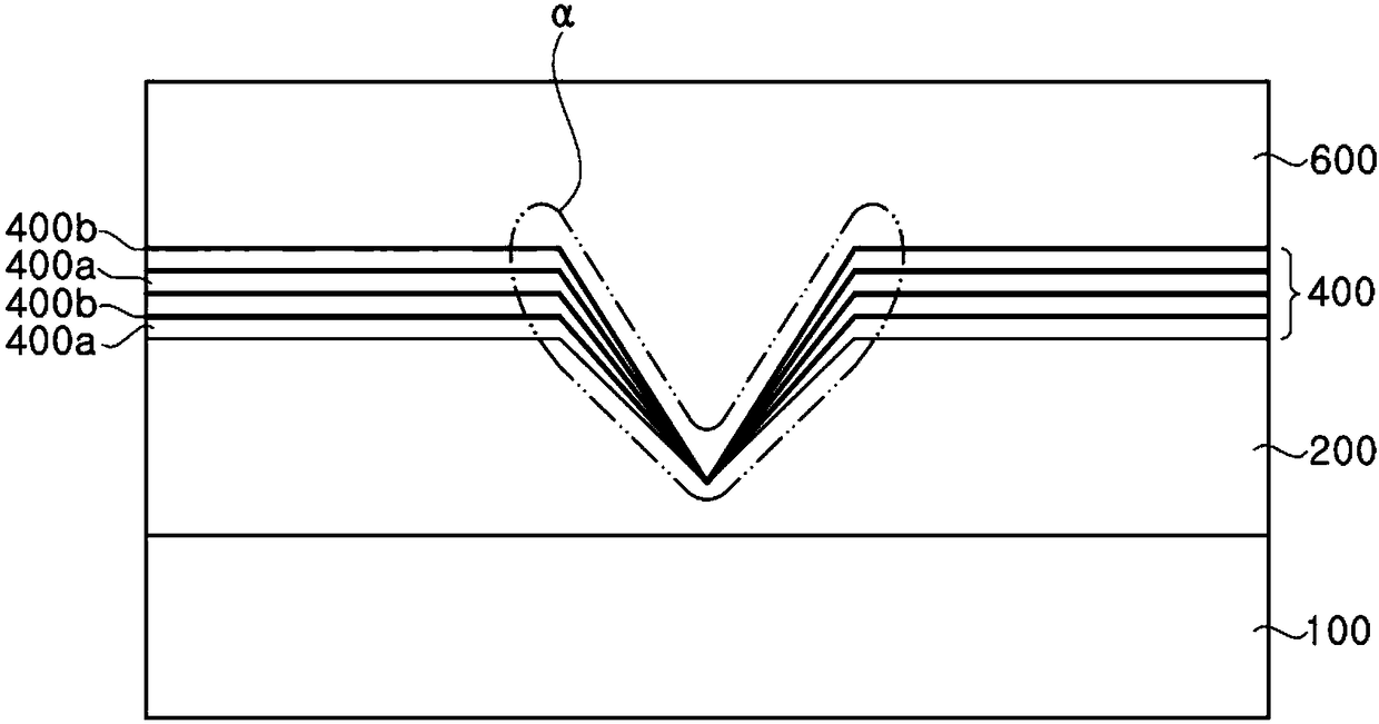
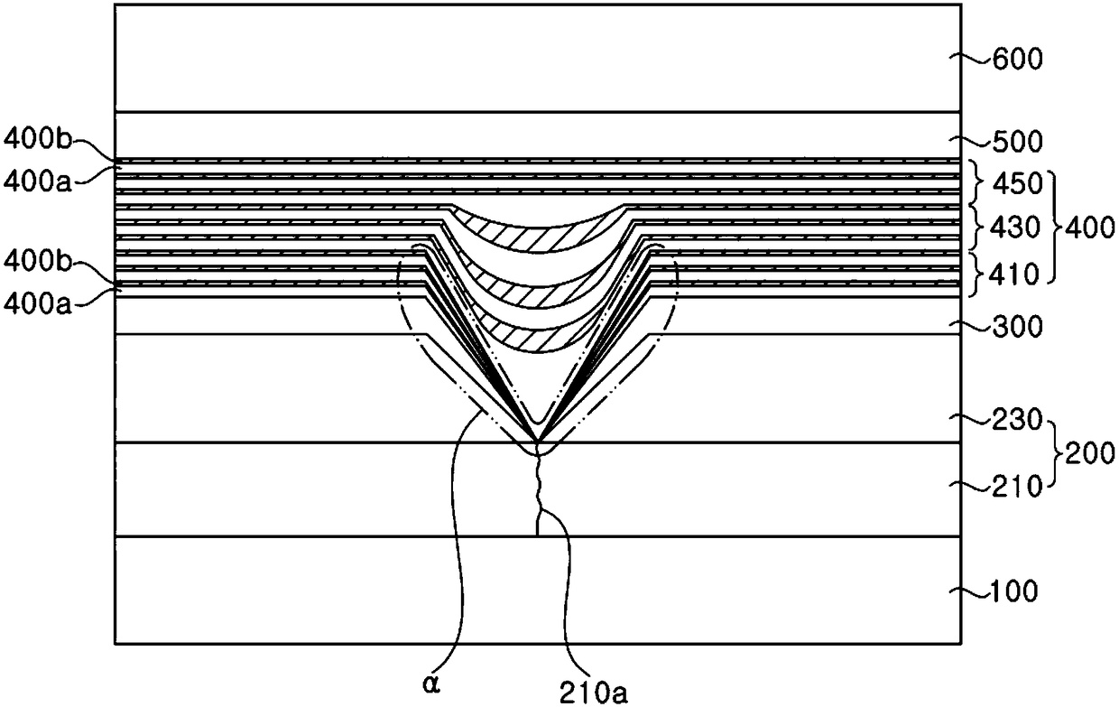
[0014] The following embodiments are provided as examples in order to fully convey the idea of ​​the present invention to those skilled in the art. Therefore, the present invention is not limited to the following examples, and may be embodied in other forms. In addition, in the drawings, the width, length, thickness, and the like of constituent elements may be exaggerated for convenience. In addition, when it is stated that a certain constituent element is located "on" or "on" another constituent element, it includes not only the case where each part is located "directly" on "on" or "on" another constituent element, but also includes A situation where another constituent element is interposed between each constituent element and another constituent element. Throughout the specification, the same reference numerals denote the same constituent elements.

[0015] According to the semiconductor light-emitting element of the present invention, it is characterized in that it compr...


PUM


Abstract

Described herein is a semiconductor light emitting device. The semiconductor light emitting device according to one embodiment comprises: an n-type semiconductor layer; a V-pit formed through at leastpart of the n-type semiconductor layer; an active layer disposed on the n-type semiconductor layer and filling the V-pit; and a p-type semiconductor layer disposed on the active layer, wherein the active layer includes a plurality of layers and part of the plural layers has a flat shape on the V-pit.

Description

technical field [0001] The invention relates to a semiconductor light-emitting element, in particular to a semiconductor light-emitting element with improved electrostatic discharge characteristics. Background technique [0002] In consideration of economic efficiency and the like, a different substrate is generally used to grow a nitride-based semiconductor layer. For example, a sapphire substrate is widely used to grow nitride-based semiconductor layers. For a nitride-based semiconductor layer grown using a heterogeneous substrate, strain may be generated due to a difference in lattice constant between the substrate and the growth layer, and thus crystal defects may be generated. In particular, threading dislocations in crystal defects may cause leakage and weak antistatic properties, and ultimately, may reduce the reliability of semiconductor light-emitting devices. [0003] The conditions for growing the nitride-based semiconductor layer are adjusted so that a V-shaped...

Claims


Application Information

Patent Timeline
Patent Type & Authority Applications(China)
IPC IPC(8): H01L33/24H01L33/14H01L33/06H01L33/32H01L33/00
CPCH01L33/0075H01L33/06H01L33/145H01L33/24H01L33/32H01L33/025H01L33/20H01L33/0008H01L33/04H01L33/16H01L2924/12041H01L33/14H01L33/12H01L33/22H01L33/02
Inventor 朴承喆郭雨澈尹俊皓
Owner SEOUL VIOSYS CO LTD
Why Eureka
Try Eureka