Unlock instant, AI-driven research and patent intelligence for your innovation.

OLED display substrate, manufacturing method thereof and display device

A display substrate and manufacturing method technology, applied in semiconductor/solid-state device manufacturing, organic semiconductor devices, electrical components, etc., can solve the problems of inverted OLED display substrate efficiency, color gamut, sacrifice of color purity, low reflectivity, etc. Achieve the effects of improving light extraction efficiency, narrowing the spectrum, and improving luminous efficiency

Active Publication Date: 2018-09-28
BOE TECH GRP CO LTD
View PDF8 Cites 4 Cited by
  • Summary
  • Abstract
  • Description
  • Claims
  • Application Information

AI Technical Summary

Problems solved by technology

However, the anode of the inverted OLED display substrate uses composite films such as ITO and IZO with high transmittance, which will lead to sacrifices in the efficiency, color gamut, and color purity of the inverted OLED display substrate.
This is because thin films such as ITO and IZO have high light transmittance, so the reflectivity is very low

Method used


Image

  • OLED display substrate, manufacturing method thereof and display device
  • OLED display substrate, manufacturing method thereof and display device
  • OLED display substrate, manufacturing method thereof and display device

Examples


Embodiment 1

[0121] The manufacturing method of the OLED display substrate of this embodiment includes the following steps:

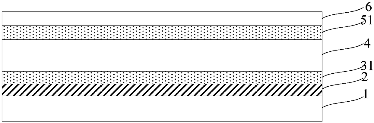
[0122] Step 1. Fabricate the driving circuit and the light-reflecting cathode layer 5 on the cleaned substrate. The light-reflecting cathode layer 5 is made of metal, and the thickness of the cathode needs to be ≥ 100 nm, so that the light-reflecting cathode layer 5 has a high reflectivity;

[0123] Step 2, using methods such as vacuum evaporation or inkjet printing to fabricate the organic light-emitting layer 4, including the OLED functional layer and the light-emitting layer. OLED functional layers usually include hole injection layer (HIL), hole transport layer (HTL), electron blocking layer (EBL), hole blocking layer (HBL), electron transport layer (ETL), electron injection layer (EIL), etc. ; The light-emitting layer includes a red light-emitting layer (REML), a green light-emitting layer (GEML), and a blue light-emitting layer (BEML);

[0124] Step 3, using ...

Embodiment 2

[0128] The manufacturing method of the OLED display substrate of this embodiment includes the following steps:

[0129] Step 1. Fabricate the driving circuit and the light-reflecting cathode layer 5 on the cleaned substrate. The light-reflecting cathode layer 5 is made of metal, and the thickness of the cathode needs to be ≥ 100 nm, so that the light-reflecting cathode layer 5 has a high reflectivity;

[0130] Step 2, using methods such as vacuum evaporation or inkjet printing to fabricate the organic light-emitting layer 4, including the OLED functional layer and the light-emitting layer. The OLED functional layer usually includes a hole injection layer, a hole transport layer, an electron blocking layer, a hole blocking layer, an electron transport layer, an electron injection layer, etc.; the light emitting layer includes a red light emitting layer, a green light emitting layer, and a blue light emitting layer;

[0131] Step 3. Prepare the transparent anode layer 3 by means...


PUM


Abstract

The invention provides an OLED display substrate, a manufacturing method thereof and a display device, belonging to the technical field of display. The OLED display substrate comprises a reflective cathode layer, an organic light emitting layer, a transparent anode layer and a high-reflecting layer that are sequentially arranged on the substrate, wherein the reflectivity of the high-reflecting layer is greater than a preset threshold. According to the technical scheme of the invention, the luminous efficiency, color gamut and color purity of an inverted OLED display substrate can be improved.

Description

technical field [0001] The invention relates to the field of display technology, in particular to an OLED display substrate, a manufacturing method thereof, and a display device. Background technique [0002] At present, an active matrix organic light emitting diode (AMOLED) display device usually consists of a reflective layer on a substrate, an anode, an organic light emitting layer, a cathode and an encapsulation layer, wherein the organic light emitting layer includes a hole injection layer (HIL), Hole Transport Layer (HTL), Electron Blocking Layer (EBL), Emissive Layer (EML), Electron Transport Layer (ETL) and Electron Injection Layer (EIL). Since the cathode needs to select a metal material with a low work function, and the reflectance of the metal material to the external ambient light is high, the contrast ratio of the display device is reduced. In addition, the transmittance of the metal cathode is low, so the thickness of the cathode is usually designed to be very...

Claims


Application Information

Patent Timeline
Patent Type & Authority Applications(China)
IPC IPC(8): H01L51/52H01L51/56
CPCH10K59/876H10K59/878H10K59/8052H10K59/8731H10K50/82H10K50/81H10K50/844H10K50/856H10K71/00H10K2102/00H10K2102/103H10K2102/321H10K2102/351H10K2102/3035
Inventor 李彦松吴海东李娜杜小波文官印樊星
Owner BOE TECH GRP CO LTD