Preparation and application of broadband light metamaterial wave-absorbing structure
A technology of metamaterials and wave structures, applied in electrical components, magnetic/electric field shielding, screening casings, etc., can solve the problems of light weight of broadband absorbing and absorbing materials, narrow absorption frequency band, etc., and achieve novel design concepts and absorbing waves Broadband, easy-to-control effects
- Summary
- Abstract
- Description
- Claims
- Application Information
AI Technical Summary
Problems solved by technology
Method used
Image

Examples
Embodiment 1
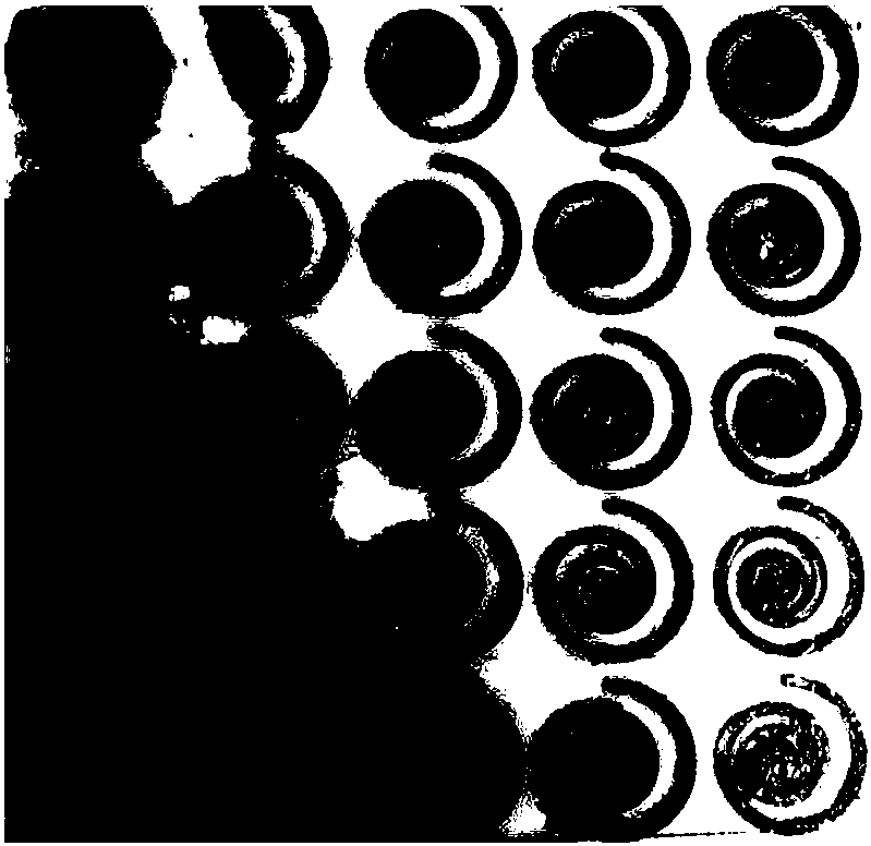
[0050] First use DXP software to design a 5×5 “mosquito-repellent incense” pattern, connect it to a fully automatic drilling, milling and engraving machine, and make a 2.0mm thick 180×180mm 2 The FR4 substrate is fixed in the engraving area for hollow engraving; then the expanded graphite is evenly mixed with a certain mass of molten paraffin at a mass fraction of 10% to obtain a microwave absorbing material; then the microwave absorbing material is filled into the hollow pattern of the FR4 substrate In the gap, the material of the broadband light-weight metamaterial wave-absorbing structure is obtained.
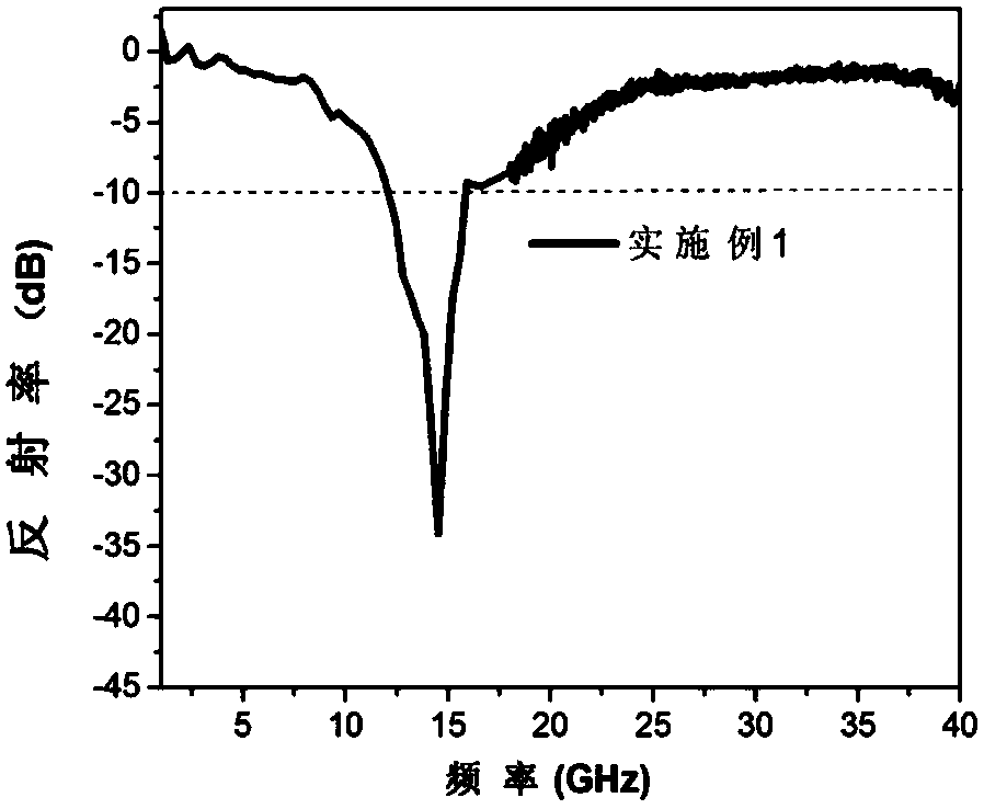
[0051] Use the material testing system to test the reflectivity (representing the absorbing performance) of the material of the broadband lightweight metamaterial absorbing structure, and the test results are as follows figure 1 – figure 2 shown. It can be seen that the frequency bandwidth of the metamaterial absorbing structure less than -10dB is about 3.8GHz, and the st...
Embodiment 2
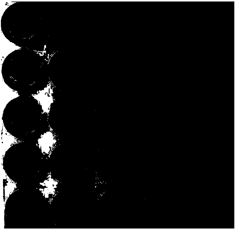
[0053] The steps are the same as in Example 1, but 1.0 mm thick FR4 material is selected as the substrate. The metamaterial absorbing structure and test reflectivity results are as follows: image 3 – Figure 4 shown. It can be seen that the frequency bandwidth of the metamaterial absorbing structure less than -10dB is about 6.9GHz, and the strongest absorption peak is -16.6dB. The surface density of the absorbing structure is 0.139kg m -2 .
Embodiment 3
[0055] The steps are the same as in Example 2, but the mass fraction of expanded graphite is 15%, and the metamaterial wave-absorbing structure and test reflectivity results are as follows Figure 5 – Figure 6 shown. It can be seen that the frequency bandwidth of the metamaterial absorbing structure less than -10dB is about 10.8GHz, and the strongest absorption peak is -29.2dB. The surface density of the absorbing structure is 0.163kg m -2 .
PUM
| Property | Measurement | Unit |
|---|---|---|
| Effective bandwidth | aaaaa | aaaaa |
| Thickness | aaaaa | aaaaa |
Abstract
Description
Claims
Application Information