
Image pickup device, image pickup display system, and display device

A camera device and a technology of the device department, applied in the direction of measuring devices, radiation control devices, TV system components, etc., can solve the problems of image degradation, image edge sensitivity reduction, etc., and achieve easy maintenance of concave shape, suppression of image quality degradation, Effect of suppressing functional deterioration

Inactive Publication Date: 2018-09-28
SONY CORP
View PDF6 Cites 0 Cited by
  • Summary
  • Abstract
  • Description
  • Claims
  • Application Information

AI Technical Summary

Problems solved by technology

For this kind of imaging device, it maintains a predetermined distance from the radiation source when imaging the target. Since the imaging device is a certain distance away from the radiation source, the sensitivity of the edge of the image is reduced, resulting in image degradation.

Method used


Image

  • Image pickup device, image pickup display system, and display device
  • Image pickup device, image pickup display system, and display device
  • Image pickup device, image pickup display system, and display device

Examples


Deformed example 1

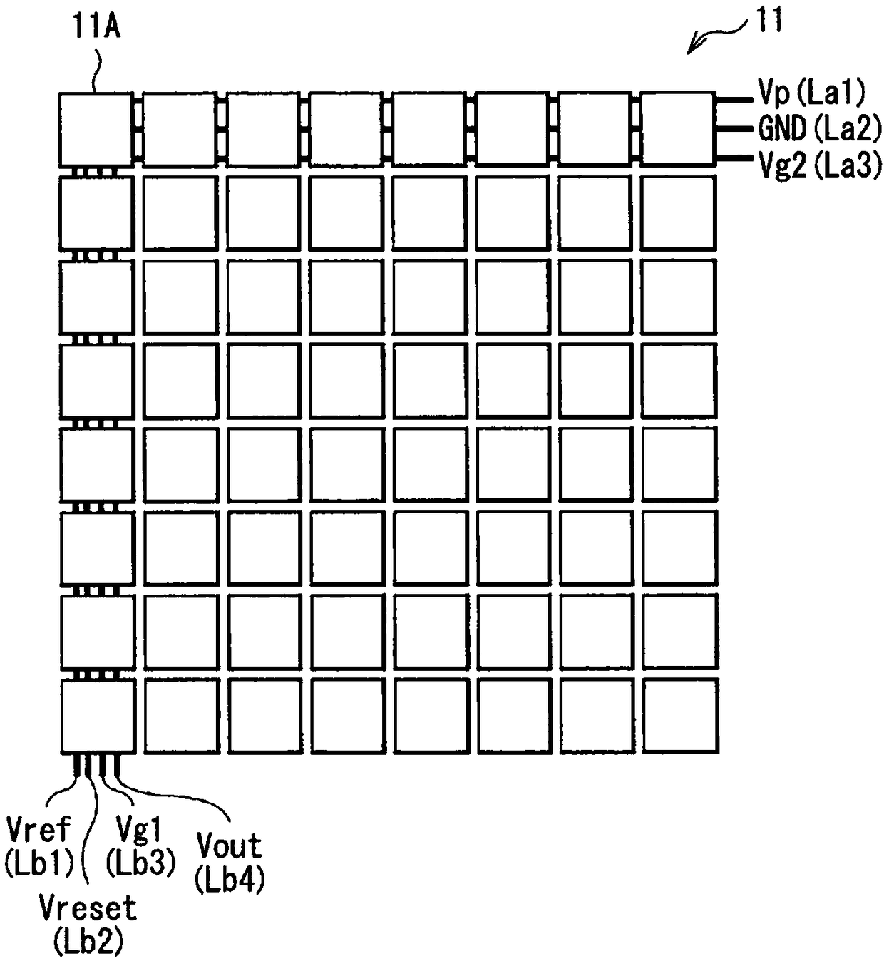
[0078] Figure 13 The functional configuration of the imaging device (imaging device 4 ) according to Modification 1 is shown. Although the description of the above-described embodiment refers to the configuration in which the pixel array section 11 includes active pixel circuits, in this modified example, the pixel array section 11 includes so-called passive pixel circuits. The imaging device 4 includes, for example, a pixel array section 11 on a substrate 410 and a driver for driving the pixel array section 11 . The driver includes, for example, a row scanner 430 , a horizontal selector 440 , a column scanner 450 and a system controller 460 .

[0079] In the pixel array section 11, like the above-described embodiments, a plurality of device sections 11A are arranged in a matrix. Pixel drive lines 470 extending in the row direction and vertical signal lines 480 extending in the column direction are connected to the device portion 11A. Each vertical signal line 480 transmit...

Deformed example 2

[0091] Figure 16 A specific configuration example of a display device (display device 2 ) according to Modification 2 is shown. Although the above-described embodiments have been described with regard to configuration examples of image pickup devices in which the pixel array portion has a concave shape, the pixel array portion of such a configuration is applicable not only to image pickup devices but also to display devices.

[0092] The display device 2 includes, for example, a pixel array section 21 having a plurality of display pixels (device section 21A) arranged two-dimensionally on a wiring substrate 20 . The wiring substrate 20 includes a plurality of wiring layers (wiring layers 231 ) on a substrate 20 a made of, for example, glass, silicon (Si), organic resin, or the like.

[0093] The plurality of device sections 21A each include a light emitting device such as a light emitting diode (LED), and are arranged spaced apart from each other (with a gap between the devic...


PUM


Abstract

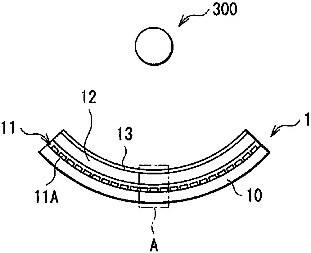
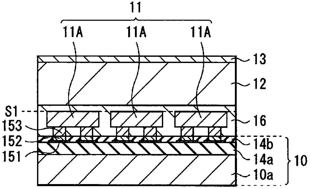
An image pickup device of the present invention is provided with: a substrate; and a plurality of element sections, which include photoelectric conversion elements, respectively, and which are disposed on the substrate by being separated from each other, said photoelectric conversion elements forming a recessed shape as a whole.

Description

technical field [0001] The present invention relates to an imaging device, an imaging display system, and a display device that detect radiation such as alpha rays, beta rays, gamma rays, or x-rays. Background technique [0002] Amorphous silicon is used in many imaging devices used in large flat panel detectors (FPD, flat panel detector) for imaging such as breasts. For such an imaging device, it maintains a predetermined distance from the radiation source when imaging a target. Since the imaging device is a certain distance away from the radiation source, the sensitivity of the edge of the image decreases, resulting in image degradation. [0003] Therefore, for example, PTL1 proposes a technique of suppressing the reduction in resolution as described above using a surface-shaped optical fiber plate. [0004] Citation list [0005] patent documents [0006] PTL 1: Japanese Patent Application Laid-Open No. H09-112301 Contents of the invention [0007] However, with the...

Claims


Application Information

Patent Timeline
Patent Type & Authority Applications(China)
IPC IPC(8): H01L27/144H01L33/00H04N5/369G01T1/20H01L27/14H01L31/02H01L31/08
CPCH01L27/14607H01L2924/181H01L2224/81203H01L2224/81444H01L2224/81455H01L2224/81469H01L2224/81801H01L24/13H01L24/16H01L24/81H01L27/14636H01L27/14663H01L27/14685H01L2224/13111H01L2224/13116H01L2224/16227H01L2224/81815H04N25/70G01T1/20189G01T1/20187G01T1/20188H01L2924/00012H01L2924/00014H01L27/144H01L31/02H01L31/08H01L27/14H01L25/041H01L21/4853H01L23/5387H01L25/0655H01L25/50H01L27/14609H01L27/14618H01L27/14629H01L31/03762H01L2224/81201
Inventor 松本一治柳川周作五十岚崇裕一木洋
Owner SONY CORP
Learn More