Thin film transistor, manufacturing method thereof and display panel

A technology for thin film transistors and a manufacturing method, which is applied in the fields of transistors, semiconductor/solid-state device manufacturing, semiconductor devices, etc., can solve the problems of increasing the leakage current of thin film transistors, high power consumption of display panels, and poor stability of thin film transistors, etc. The effect of leakage current, reducing power consumption and improving electrical performance stability

Inactive Publication Date: 2018-10-02
HKC CORP LTD +1
View PDF3 Cites 3 Cited by
  • Summary
  • Abstract
  • Description
  • Claims
  • Application Information

AI Technical Summary

Problems solved by technology

[0003] The display panel is provided with a thin-film transistor array substrate, but the leakage current of the thin-film transistors in the existing thin-film transistor array substrate is relatively large, and when light is irradiated on the thin-film transistor, photo-generated carriers will be generated, further increasing the density of the thin-film transistor. Leakage current, resulting in large power consumption of the display panel, and poor stability of thin film transistors

Method used


Image

  • Thin film transistor, manufacturing method thereof and display panel
  • Thin film transistor, manufacturing method thereof and display panel
  • Thin film transistor, manufacturing method thereof and display panel

Examples


Embodiment Construction

[0028] In order to make the purpose, technical solutions and advantages of the present invention clearer, the technical solutions of the present invention will be clearly and completely described through implementation with reference to the accompanying drawings in the embodiments of the present invention. Obviously, the described embodiments are the embodiment of the present invention. Some, but not all, embodiments. Based on the embodiments of the present invention, all other embodiments obtained by persons of ordinary skill in the art without making creative efforts belong to the protection scope of the present invention.

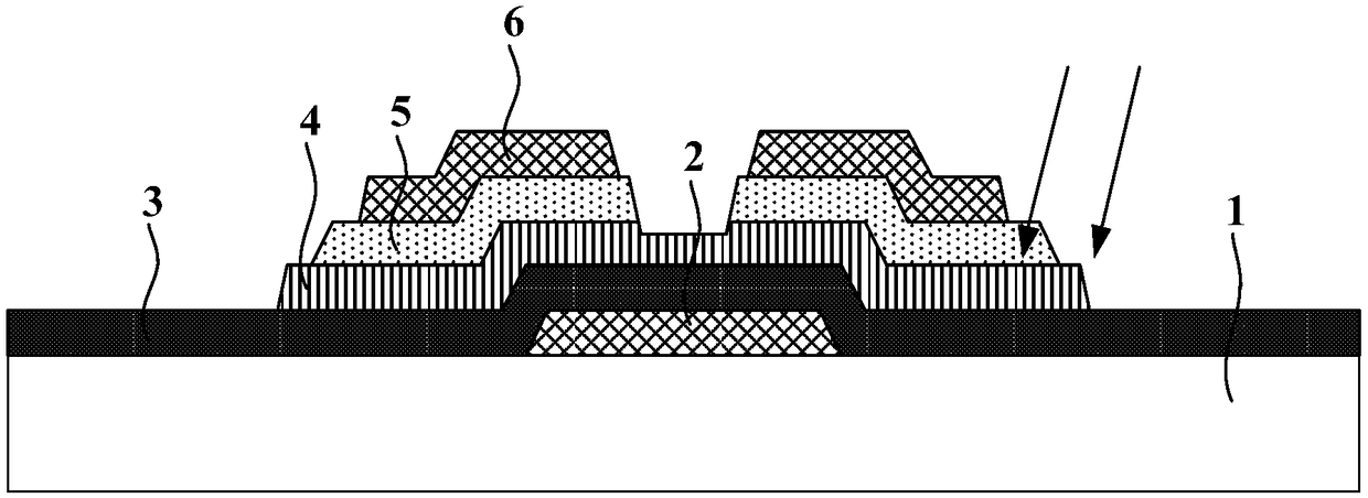
[0029] refer to figure 1 Shown is an exemplary thin film transistor provided. The thin film transistor is manufactured by using a 4-pass mask process, that is, a 4-mask process. Specifically, the thin film transistor includes: a substrate 1, a gate 2, a gate insulating layer 3, an amorphous silicon layer 4, a doped layer 5 and Source and drain 6. In t...


PUM


Abstract

The embodiment of the invention discloses a thin film transistor, a manufacturing method thereof and a display panel. The thin film transistor comprises a substrate, a gate, a gate insulation layer, asemiconductor layer, a doping layer and a source-drain, wherein the gate, the gate insulation layer, the semiconductor layer, the doping layer and the source-drain are sequentially formed on the substrate, and the semiconductor layer is used for absorbing a light ray with wavelength larger than 760 nanometers. In the thin film transistor disclosed by the embodiment of the invention, the light raycannot be absorbed by the semiconductor layer of the thin film transistor due to the characteristic that visible light is not absorbed by the semiconductor layer even the light ray radiates the semiconductor layer of the thin film transistor, the light ray cannot react with the visible light to generate a light leakage current, so that the leakage current of the thin film transistor cannot be increased. Compared with the prior art, the leakage current of the thin film transistor is reduced, the electrical performance stability of the thin film transistor is improved, and the power consumptionof the display panel also can be reduced when the thin film transistor is applied to the display panel.

Description

technical field [0001] Embodiments of the present invention relate to transistor technology, and in particular to a thin film transistor, a manufacturing method thereof, and a display panel. Background technique [0002] Thin-film transistors are the key components of display panels, which play a very important role in the performance of display panels. With the rapid development of electronic equipment, people require that the power consumption of electronic equipment should be as low as possible, and the battery life should be as high as possible. Therefore, Low power consumption of display panels in electronic equipment is also required. [0003] The display panel is provided with a thin-film transistor array substrate, but the leakage current of the thin-film transistors in the existing thin-film transistor array substrate is relatively large, and when light is irradiated on the thin-film transistor, photo-generated carriers will be generated, further increasing the dens...

Claims


Application Information

Patent Timeline
Patent Type & Authority Applications(China)
IPC IPC(8): H01L29/786H01L21/336
CPCH01L29/66765H01L29/78609H01L29/78678H01L29/78684
Inventor 卓恩宗
Owner HKC CORP LTD
Why Eureka
Try Eureka