A kind of pcb solder resist pattern manufacturing method and pcb

A production method and solder mask technology, applied in the manufacturing of printed circuits, printed circuits, electrical components, etc., can solve the problems of ink being easily washed off, the thickness of the ink is not up to standard, and the ink is easily washed away, so as to improve the quality and product quality. Reliability, solving false copper exposure, solid curing effect

Active Publication Date: 2020-02-11
SHENZHEN SHIRUITAI TECH
View PDF5 Cites 0 Cited by
  • Summary
  • Abstract
  • Description
  • Claims
  • Application Information

AI Technical Summary

Problems solved by technology

[0003] In the above-mentioned prior art, the solder resist ink is only in a light-cured state after exposure, and the hardness and developer resistance of the ink are insufficient. In the subsequent developing process, the developing solution washes the board surface. The ink in the through hole on the board is easy to be washed off, and the ink on the edge of the through hole is also easily washed off, resulting in no ink coverage on the edge of the through hole or the thickness of the ink is not up to standard, resulting in no ink around the through hole Covering causes the copper surface to be exposed, commonly known as false copper leakage

Method used


Image

  • A kind of pcb solder resist pattern manufacturing method and pcb

Examples


Embodiment Construction

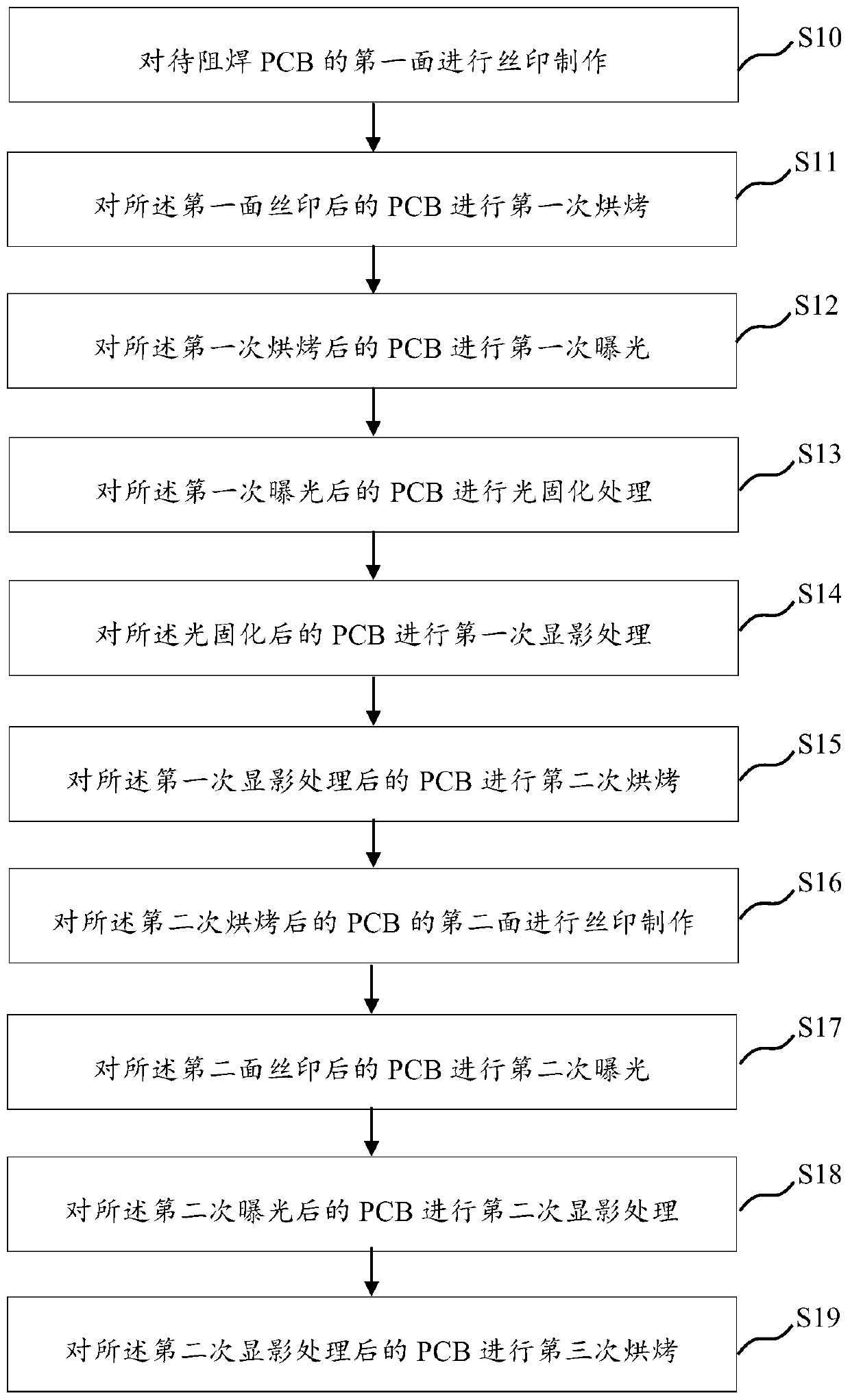
[0020] The following will clearly and completely describe the technical solutions in the embodiments of the present invention with reference to the accompanying drawings in the embodiments of the present invention. Obviously, the described embodiments are some of the embodiments of the present invention, but not all of them. Based on the embodiments of the present invention, all other embodiments obtained by persons of ordinary skill in the art without making creative efforts belong to the protection scope of the present invention.

[0021] It should be understood that when used in this specification and the appended claims, the terms "comprising" and "comprises" indicate the presence of described features, integers, steps, operations, elements and / or components, but do not exclude one or Presence or addition of multiple other features, integers, steps, operations, elements, components and / or collections thereof.

[0022] It should also be understood that the terminology used ...


PUM


Abstract

The invention discloses a welding-resistant pattern fabrication method of a PCB and the PCB. The method comprises the following steps of performing silk-screen fabrication on a first surface of the PCB to be resistant-welded, performing first-time baking on the PCB after silk-screen on the first surface, performing first-time exposure on the PCB after first-time baking, performing photocuring on the PCB after first-time exposure, performing first-time developing on the PCB after photocuring, performing second-time baking on the PCB after first-time developing, performing silk-screen fabrication on a second surface of the PCB after second-time baking, performing second-time exposure on the PCB after silk-screen on the second surface, performing second-time developing on the PCB after second-time exposure, and performing third-time baking on the PCB after second-time developing. By the method, the problem of pseudo copper leakage of a PCB product with relatively small thickness (e.g. thethickness is smaller than or equal to 0.7 millimeters) during the welding-resistant pattern fabrication process can be solved, and the reliability of the PCB product is improved.

Description

technical field [0001] The invention relates to the field of electronic manufacturing, in particular to a method for manufacturing a PCB solder resist pattern and a PCB. Background technique [0002] For products with a small overall board thickness in the PCB (Printed Circuit Board, printed circuit board) industry, such as printed circuit boards with a board thickness ≤ 0.7mm or FPC (Flexible Printed Circuit, flexible printed circuit board) and soft and hard boards Generally, the following three methods are used to make solder resist patterns: 1. Double-sided silk screen printing method is used. The process is roughly as follows: silk screen A side → flip → use nail bed to support screen B side → pre-baking → alignment → exposure → development, corresponding The exposure process uses double-sided film for one exposure, and the corresponding exposure process uses double-sided film for one exposure; 2. The method of single-side printing solder mask and single-side exposure is...

Claims


Application Information

Patent Timeline
Patent Type & Authority Patents(China)
IPC IPC(8): H05K3/28
CPCH05K3/282H05K2203/052
Inventor 李达林王文剑陈国忠余宁
Owner SHENZHEN SHIRUITAI TECH
Why Eureka
Try Eureka