Field-effect transistor structure with multiple gate changes, its manufacturing method, and chip device

A technology for field effect transistors and manufacturing methods, applied in the field of field effect transistor structures with variable gates and its manufacture, and chip devices, can solve the incompatibility of product performance and reliability, and the uneven distribution of source electron currents of field effect transistors Uniformity, incompatibility between product performance and processing difficulty, etc., to reduce production line switching costs, improve process commonality, and increase vertical channel arrangement density

Active Publication Date: 2022-05-17
深圳真茂佳半导体有限公司
View PDF14 Cites 0 Cited by
  • Summary
  • Abstract
  • Description
  • Claims
  • Application Information

AI Technical Summary

Problems solved by technology

[0005] The main purpose of the present invention is to provide a field effect transistor structure with multi-gate changes. The main progress is to solve the problem of uneven distribution of source electron current, product performance and reliability incompatibility, and product The problem of incompatibility between performance and processing difficulty

Method used


Image

  • Field-effect transistor structure with multiple gate changes, its manufacturing method, and chip device
  • Field-effect transistor structure with multiple gate changes, its manufacturing method, and chip device
  • Field-effect transistor structure with multiple gate changes, its manufacturing method, and chip device

Examples


Embodiment Construction

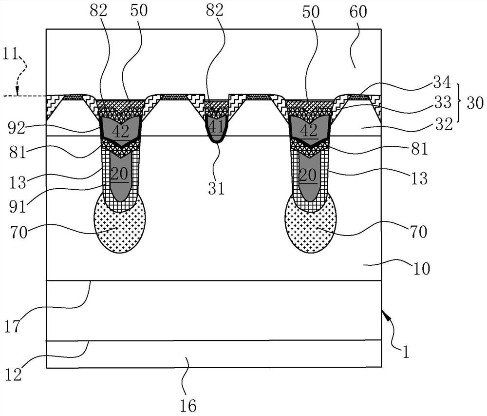
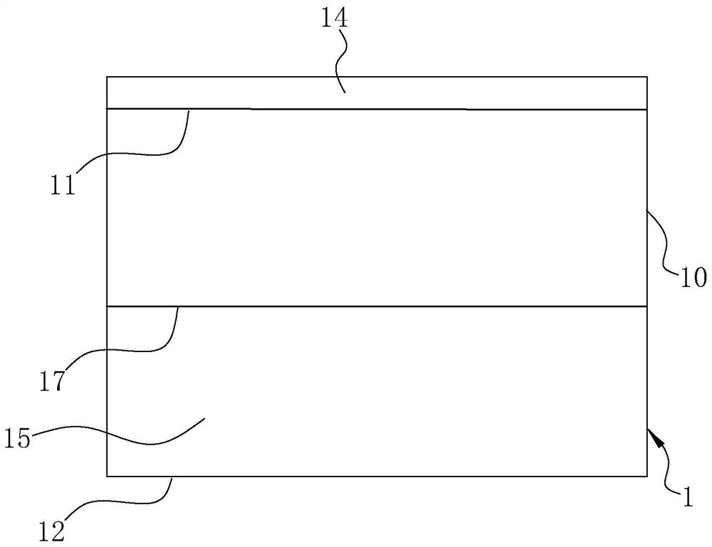
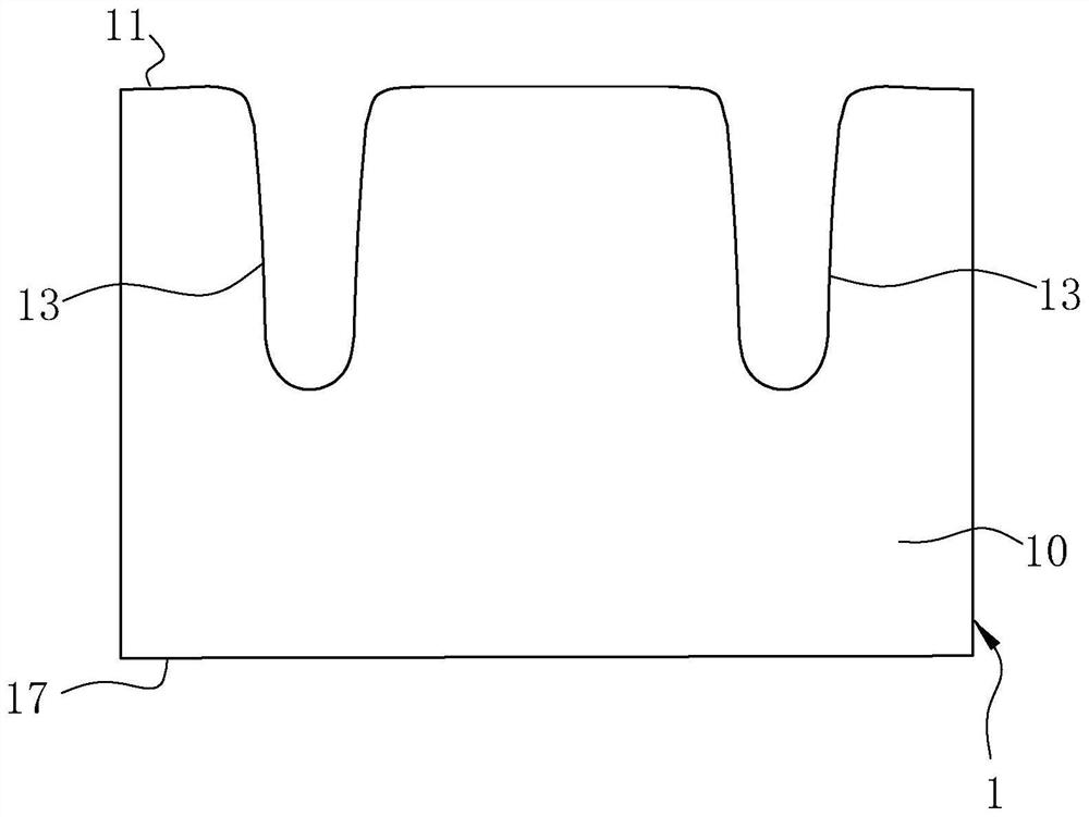
[0083] The technical solutions in the embodiments of the present invention will be clearly and completely described below in conjunction with the accompanying drawings in the embodiments of the present invention. Apparently, the described embodiments are only part of the embodiments for understanding the inventive concepts of the present invention, and cannot represent All the embodiments are not explained as the only embodiment. Based on the embodiments of the present invention, all other embodiments obtained by persons of ordinary skill in the art on the premise of understanding the inventive concepts of the present invention fall within the protection scope of the present invention.

[0084] It should be noted that if there is a directional indication (such as up, down, left, right, front, back...) in the embodiment of the present invention, the directional indication is only used to explain the relationship between the components in a certain posture. If the specific postu...


PUM


Abstract

The present invention relates to a multi-gate variable field effect transistor structure, its manufacturing method, and chip device. The transistor includes a drain epitaxial layer on the bottom layer, a source layer on the top layer, and a source extension embedded in the drain epitaxial layer. Inverted fins, first gate and second gate; the first gate is arranged between the source extended inverted fins, the second gate is aligned on the source extended inverted fins, the first gate and the second gate A pair of symmetrical channels connected in parallel from the source layer to the drain epitaxial layer are formed on both sides of each side; in a preferred example, the drain epitaxial layer forms a floating anti-air barrier at the bottom of the extended inverted fin corresponding to the source. Pole bottom junction. The structure of the field effect transistor provided by the present invention is the densification of multi-gate changes, and has the effect of uniformizing the electron flow of the substrate backside drain and the top surface source, and the effect of reducing the slotting process.

Description

technical field [0001] The invention relates to the technical field of semiconductor transistors, in particular to a multi-gate variable field effect transistor structure, a manufacturing method thereof, and a chip device. Background technique [0002] As the key and important device of the semiconductor chip, the field effect transistor structure has a variety of structures, mainly including the following types: FinFET fin field effect transistor, JFET junction field effect transistor, surface field effect transistor, tunneling field effect transistor Transistors trench gate field effect transistor, split gate field effect transistor and super junction field effect transistor. Among them, the structure of FinFET fin field effect transistor, JFET junction field effect transistor, surface field effect transistor and tunneling field effect transistor is to design the source contact and drain contact on the same surface of the semiconductor substrate. With the trend of thinnin...

Claims


Application Information

Patent Timeline
Patent Type & Authority Patents(China)
IPC IPC(8): H01L29/06H01L29/08H01L29/10H01L29/423H01L29/78H01L21/336H01L21/28
CPCH01L29/7855H01L29/7827H01L29/401H01L29/42356H01L29/4236H01L29/1037H01L29/0623H01L29/0847H01L29/66484H01L29/66795
Inventor 任炜强
Owner 深圳真茂佳半导体有限公司
Why Eureka
Try Eureka