
Eureka
For R&D, Eureka makes reading and utilizing patents & technical documents easy.
Eureka AIR
Designed for self-driven R&D workflows. Generate viable solutions, solve complex R&D challenges, empower your innovation with AI.

Eureka Materials
Designed for material experts only. Revolutionize your material R&D, from search, analyze, to developing new materials.

TechResearch
Generate reliable direction feasibility study reports for your R&D in just a few steps.

TechSeek
Discover and master advanced knowledge NOW. Basics, ideas, possibilities, all at once.

TechMind
As an expert in R&D Theories, TechMind can generates customized viable solutions instantly.

TechRisk
Analyze your overall solution with one click, know your potential R&D risks in advance.

TechMonitor
Get weekly tech updates, stay abreast of the latest tech innovations and key insights.
Processing method
A processing method and a technology of processed objects, which are applied in the direction of electrical components, semiconductor/solid-state device manufacturing, circuits, etc., can solve the problems of rising manufacturing costs and generation of debris
- Summary
- Abstract
- Description
- Claims
- Application Information
AI Technical Summary
Problems solved by technology
Method used
Image

Examples
Embodiment approach 1
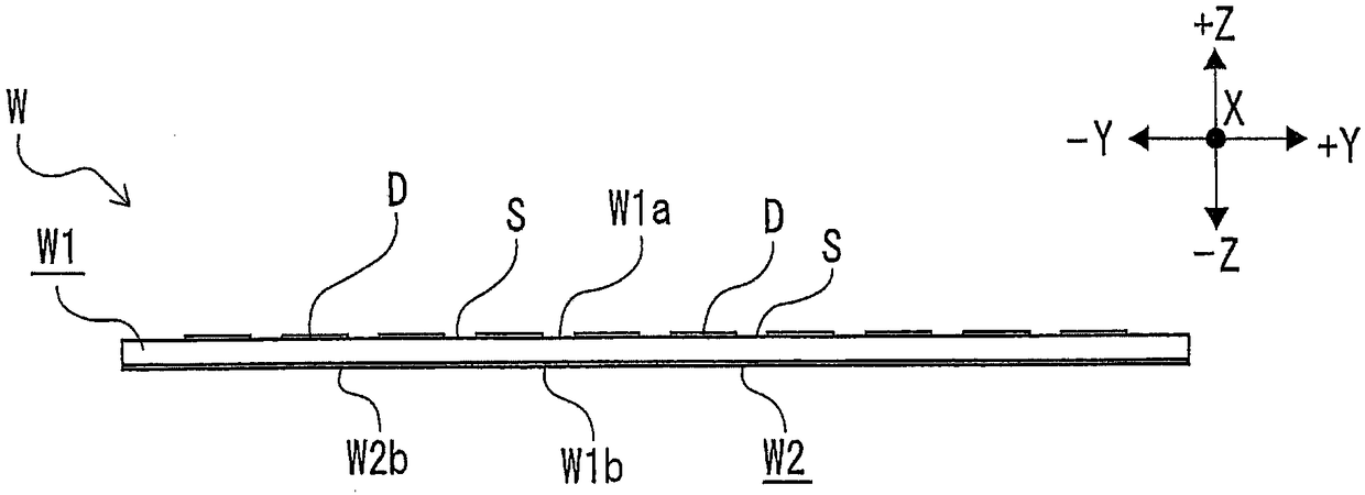
[0024] Below, implement the processing method of the present invention by figure 1 Each step of the processing method for producing a chip having the device D from the workpiece W shown will be described.
[0025] (1-1) Groove forming process using a cutting device
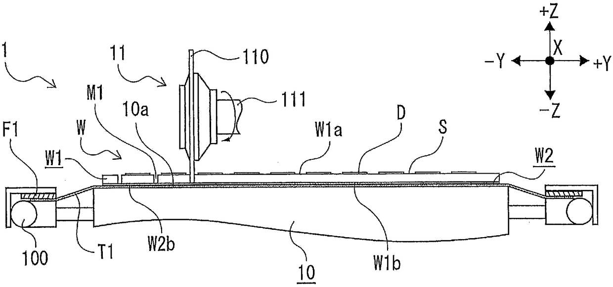
[0026] First, implement the groove forming step from figure 1 Grooves are formed on the front surface W1a of the workpiece W shown along lines S to be divided. In this groove forming step, for example, using figure 2 The cutting device 1 shown is used for groove formation.
[0027] When forming grooves, such as figure 2 As shown, the workpiece W is in the following state: a dicing tape T1 having a diameter larger than the workpiece W is attached to the back surface W2b of the workpiece W, and the outer peripheral portion of the adhesive surface of the dicing tape T1 is attached to the ring frame. on F1. And the workpiece W in the state where the front surface W1a is exposed upward is supported by the ring ...
Embodiment approach 2
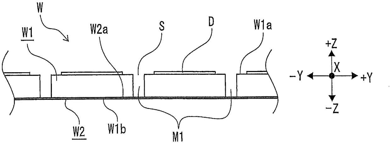
[0081] Below, implement the processing method of the present invention by figure 1 Each step of the processing method for producing a chip having the device D from the workpiece W shown will be described. In Embodiment 2 of the processing method of the present invention, as in Embodiment 1 of the processing method of the present invention, first, (1-1) a groove forming step using a cutting device or (1-2) a step of forming a groove using a plasma etching device is performed. Any step in the groove forming step such as image 3 As shown, grooves M1 whose depth does not reach the film W2 are formed on the workpiece W along all the planned dividing lines S.
[0082] (2) Hold step
[0083] After performing either of (1-1) the groove forming step using the cutting device 1 or (1-2) the groove forming step using the plasma etching device 9, as Figure 5 As shown in , stick the protective tape T3 on the front W1a of the workpiece W, and place the figure 2 Scribe Tape T1 as shown o...
PUM
 Abstract
Description
Claims
Application Information
 - R&D Engineer
- R&D Manager
- IP Professional
- Industry Leading Data Capabilities
- Powerful AI technology
- Patent DNA Extraction
Browse by: Latest US Patents, China's latest patents, Technical Efficacy Thesaurus, Application Domain, Technology Topic, Popular Technical Reports.
© 2024 PatSnap. All rights reserved.Legal|Privacy policy|Modern Slavery Act Transparency Statement|Sitemap|About US| Contact US: help@patsnap.com