Methods and Device for Laser Processing

a laser processing and laser technology, applied in the field of laser microlithography, can solve the problems of low throughput of dmd direct laser ablation, limited pulse power per mirror, and waste of most expensive materials that have been blanketed, and achieve the effect of facilitating laser ablation

Inactive Publication Date: 2011-10-06
MICRONIC LASER SYST AB
View PDF6 Cites 85 Cited by
  • Summary
  • Abstract
  • Description
  • Claims
  • Application Information

AI Technical Summary

Benefits of technology

[0013]The present invention relates to laser ablation microlithography. In particular, we disclose a new SLM design and patterning method that uses multiple mirrors per pixel to concentrate energy to an energy density that facilitates laser ablation, while keeping the energy density on the SLM mirror surface at a level that does not

Problems solved by technology

This procedure ensures high quality, but involves many steps, and in some cases, most of the expensive material that has been blanket deposited goes to waste.
The throughput for DMD direct laser ablation is low because of the moderate power density and update rate that can be achieved with a DMD.
The pulse power per mirror is limited partly by the size of the mirrors, partly by the ris

Method used


Image

  • Methods and Device for Laser Processing
  • Methods and Device for Laser Processing
  • Methods and Device for Laser Processing

Examples


example embodiment

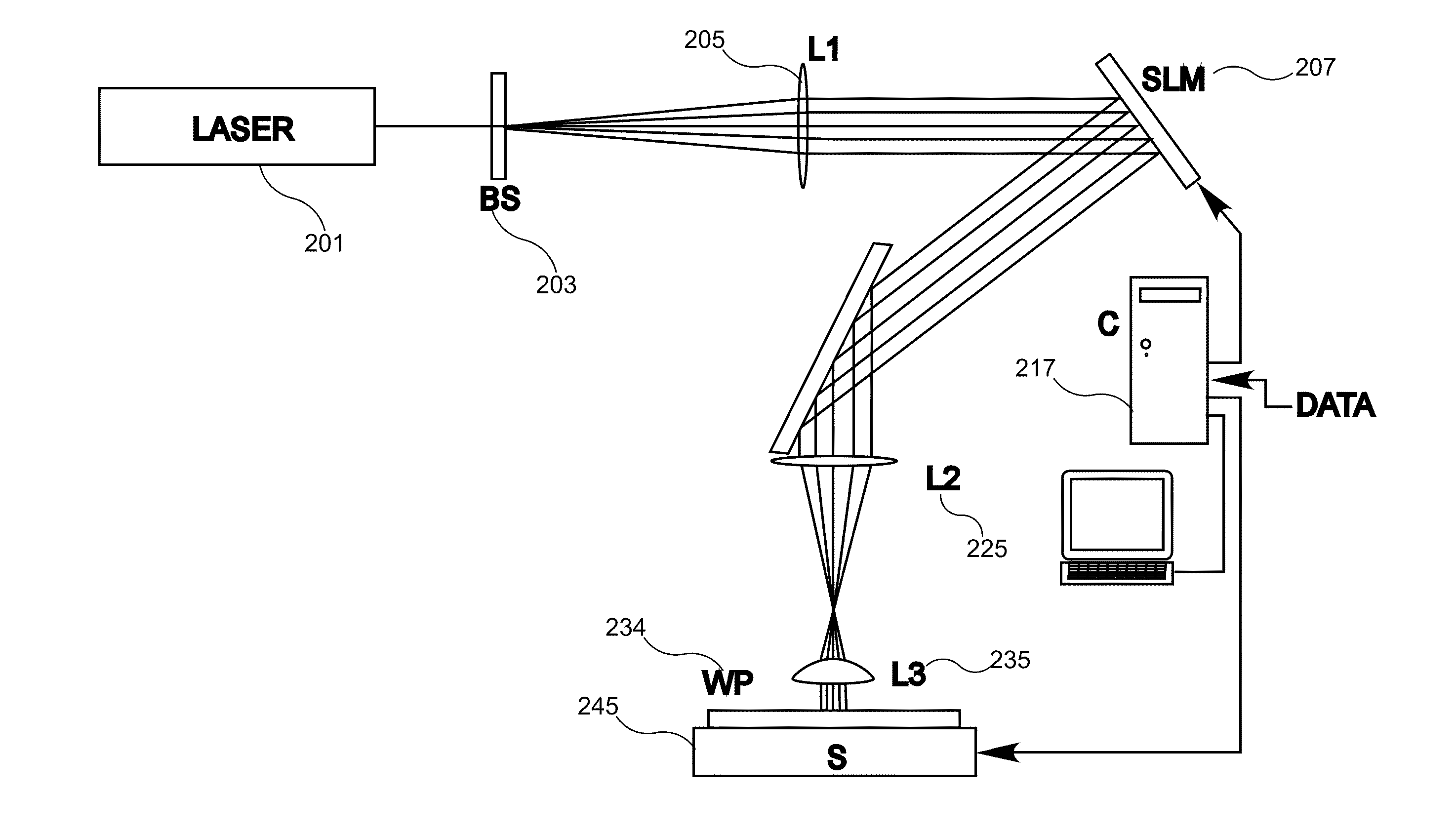
[0041]In one design, we propose using a laser with 50 W average power and 1 MHz repetition rate. The optical efficiency from laser to workpiece may be 50%. The SLM has 8192 pixels and the beam is split and focused to illuminate every third pixel. The unused pixels in between act as separation zones that keep the beamlets from interfering with one another. We have

81923=2730beams,

each with an effective footprint on the SLM of 10*1000 sq. μm, which is 0.01 sq. mm. The pulse energy per mirror is 25 w / 2730 / 1 MHz=10 nJ and the energy density is 100 μJ / sq. cm or 10,000 times too low for ablation. Therefore the mirrors are safe from the pulse energy. After demagnifying the image 40,000 times by area, i.e. making the each spot 0.5*0.5 μm sq., we arrive at 4 J / sq. cm, which is a reasonable ablation power. We now have 25 W energy ablating the workpiece and a pixel rate (number of beamlets times pulse frequency) of 2730*1,000,000=2.7 billion data pixels per second. At this rate, it is calculate...


PUM

PropertyMeasurementUnit
Timeaaaaaaaaaa
Timeaaaaaaaaaa
Timeaaaaaaaaaa

Abstract

The present invention relates to laser ablation microlithography. In particular, we disclose a new SLM design and patterning method that uses multiple mirrors per pixel to concentrate energy to an energy density that facilitates laser ablation, while keeping the energy density on the SLM mirror surface at a level that does not damage the mirrors. Multiple micro-mirrors can be reset at a very high frequency, far beyond current DMD devices.

Description

RELATED APPLICATION[0001]This application claims the benefit of U.S. Provisional Patent Application No. 61 / 311,271 entitled “Methods and Device for Laser Ablation,” filed Mar. 5, 2010. The priority application is incorporated by reference.[0002]This application is related to and incorporates by reference U.S. patent application Ser. No. 12 / 626,581, entitled “Image Reading And Writing Using A Complex Two-Dimensional Interlace Scheme,” filed on Nov. 25, 2009 [MLSE 1098-2 / P00339], which discloses methods and systems that use large SLMs with many pixels.[0003]This application is related to and incorporates by reference U.S. patent application Ser. No. 12 / 706,624, entitled “SLM Device And Method Combining Multiple Mirrors For High-Power Delivery,” filed on Feb. 16, 2010 [MLSE 1101-2 / P00346], which discloses SLMs having improved image quality, modulation speed, and power handling.[0004]This application is further related to and incorporates by reference U.S. patent application Ser. No. 12...

Claims


Application Information

Patent Timeline
IPC IPC(8): B23K26/00
CPCB23K26/032B41J2/465B23K26/0676B23K26/0807B23K26/0853B23K26/36B23K26/367B23K26/4025B23K2201/40G02B26/0841G02B27/42G03F7/70291G03F7/70875B23K26/0066B23K26/08H01L21/302B23K26/0635B23K26/364B23K26/082B23K26/0624B23K2101/40B23K2103/50B23K26/352
Inventor SANDSTROM, TORBJORN
Owner MICRONIC LASER SYST AB
Why Eureka
Try Eureka