Laser processing apparatus and laser processing method

a laser processing and processing apparatus technology, applied in metal working apparatus, manufacturing tools, welding/soldering/cutting articles, etc., can solve the problems of reducing processing efficiency and low throughput, and unsuitable for mass production, so as to achieve reliably the effect of forming a normal modifying region in a short period of tim

Inactive Publication Date: 2007-08-30
DENSO CORP
View PDF23 Cites 94 Cited by
  • Summary
  • Abstract
  • Description
  • Claims
  • Application Information

AI Technical Summary

Benefits of technology

[0029] The present invention has been made in consideration of the foregoing. Objects of the invention are as follows. (1) One object is to provide a small and low-cost laser processing apparatus capable of reliably forming a normal modifying region in a short period of time in order to form multi

Problems solved by technology

When a wafer is thick, it is technologically difficult to accurately cut and separate the wafer along an estimated cut line.
The technology shows decreased processing efficiency and low throughput (productivity per unit time) and is unsuited for mass production.
A semiconductor device may be damaged due to radiation of a laser beam to a region for forming the semiconductor device on the wafer surface.
The chip yield is limited to increase manufacturing costs for chips.
Forming multiple modifying regions is time-consuming.
The technology shows low throughput (productivity per unit time) and is unsuited for mass production.
Accordingly, the laser processing apparatus becomes large and increases an installation space.
In addition, the laser processing apparatus becomes complicated to increase the number of parts and therefore manufacturing costs.
When a wafer is very thick, it is difficult to reliably form normal modifying regi

Method used


Image

  • Laser processing apparatus and laser processing method
  • Laser processing apparatus and laser processing method
  • Laser processing apparatus and laser processing method

Examples


first embodiment

1. First Embodiment

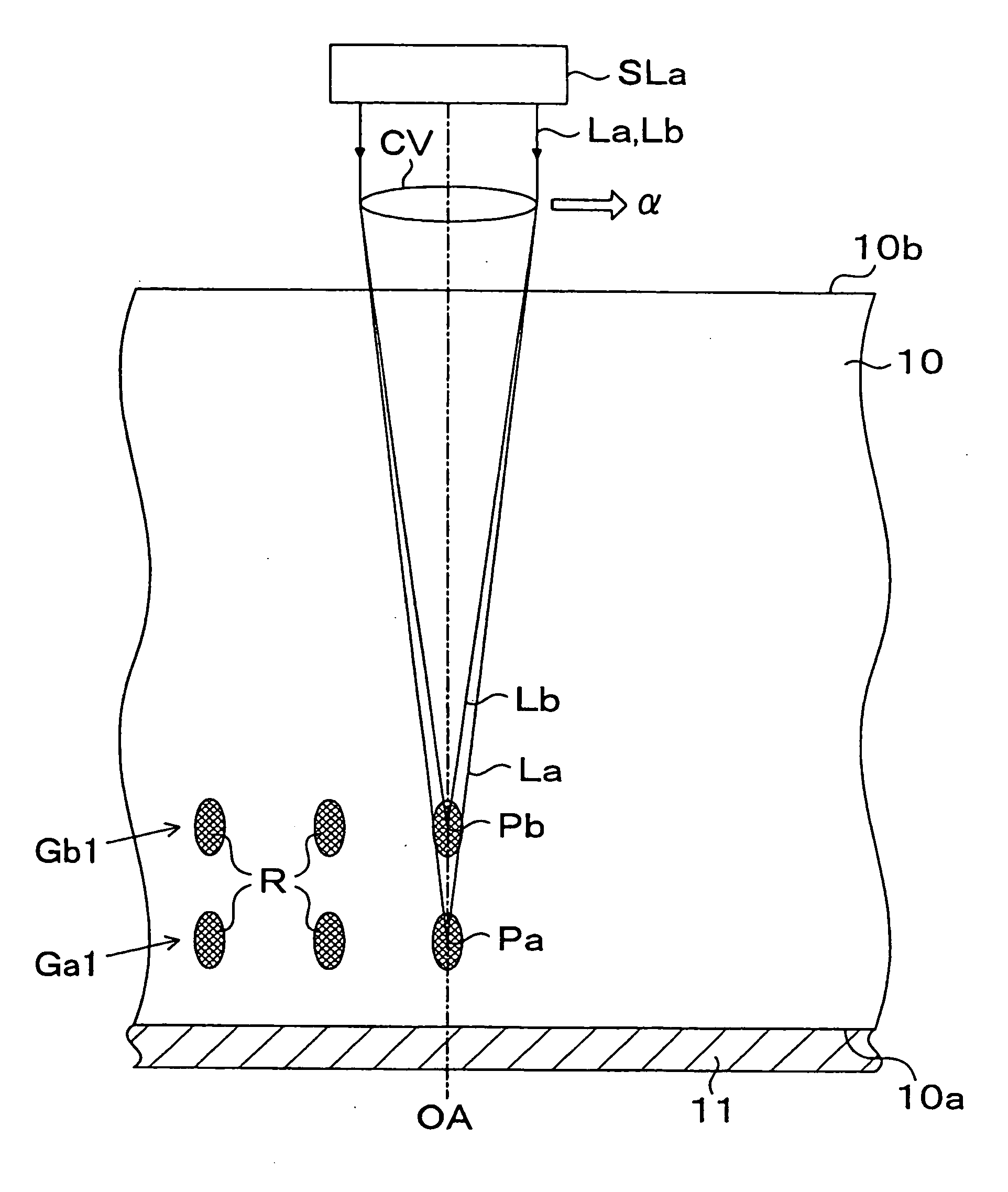
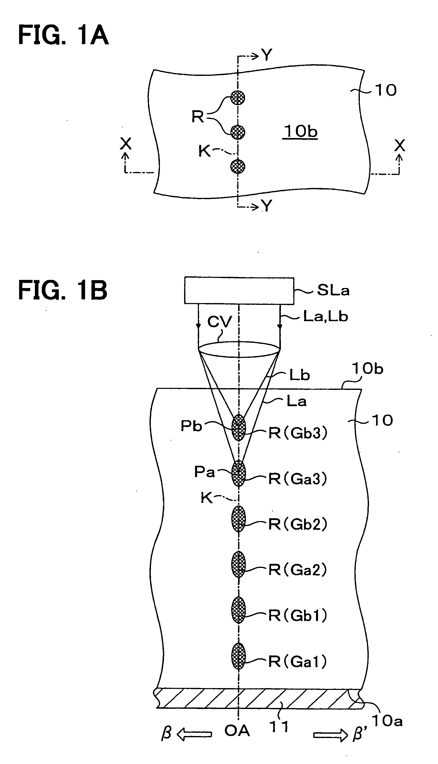
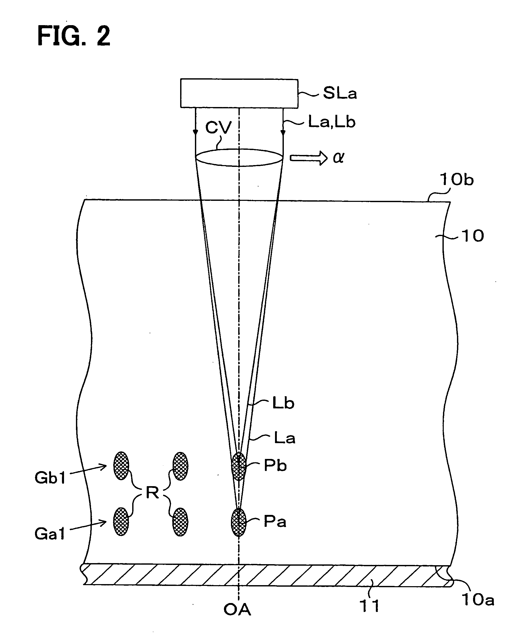
[0063]FIGS. 1A, 1B, and 2 through 4 illustrate processes to radiate a laser beam to a wafer 10 and form a modifying region according to a first embodiment. FIG. 1A shows a plan view of the wafer 10. FIGS. 1B and 2 through 4 schematically show longitudinal sectional views of the wafer 10. FIG. 1B is a sectional view taken in the line X-X of FIG. 1A. FIGS. 2 through 4 are sectional views taken in the line Y-Y of FIG. 1A equivalent to estimated cut line K.

[0064] A wafer (bulk silicon wafer) 10 is made of a bulk monocrystalline silicon material. A reverse side 10a of the wafer 10 is attached with a dicing film (dicing sheet, dicing tape, and expand tape) 11. The dicing film 11 is made of an expansible plastic film material that expands by heating or applying a force in an expanding direction. The dicing film 11 is bonded to all over the reverse side of the wafer 10 with an adhesive (not shown).

[0065]1: See FIG. 2>

[0066] The laser processing apparatus is provided wit...

second embodiment

2. Second Embodiment

[0098]FIGS. 5 and 6 illustrate processes to radiate a laser beam to the wafer 10 and form a modifying region according to a second embodiment. FIGS. 5 and 6 schematically show longitudinal sectional views of the wafer according to the second embodiment.

[0099]1: See FIG. 5>

[0100] The laser processing apparatus is provided with one laser light source SLb and one condenser lens CV The laser light source SLb selects one of a laser beam Lc with wavelength λc and a laser beam Lc with wavelength λd. The laser light source SLb then generates to radiate the laser beam with the selected wavelength.

[0101] The laser processing apparatus allows laser light source SLb to radiate laser beam Lc with wavelength λc. Optical axis OA for laser beam Lc is kept perpendicular to the surface 10b of the wafer 10. In this state, laser beam Lc is radiated to the surface 10b (incidence plane for the laser beam Lc) of the wafer 10 via condenser lens CV. Laser beam Lc is converged on focusi...

third embodiment

3. Third Embodiment

[0122]FIGS. 7 and 8 illustrate processes to radiate a laser beam to the wafers 12 and 13 and form a modifying region according to a third embodiment. FIGS. 7 and 8 schematically show longitudinal sectional views of the wafers 12 and 13 according to the third embodiment.

[0123] The wafers (bulk silicon wafer) 12 and 13 are made of a bulk monocrystalline silicon material. The dicing film 11 is bonded to a reverse side 12a of the wafer 12. The wafer 13 is layered on a surface 12b of the wafer 10. The surface 12b of the wafer 12 and the reverse side 13a of the wafer 13 are bonded to form a two-layer structure.

[0124]1: See FIG. 7>

[0125] The laser processing apparatus is provided with one laser light source SLc and one condenser lens CV The laser light source SLc selects one of laser beam Le with wavelength λe and laser beam Lf with wavelength λf. The laser light source SLc then generates to radiate the laser beam with the selected wavelength.

[0126] The laser processi...


PUM

PropertyMeasurementUnit
Timeaaaaaaaaaa
Depthaaaaaaaaaa
Wavelengthaaaaaaaaaa

Abstract

A laser processing apparatus has one laser light source that simultaneously radiates laser beams with two wavelengths. Depth positions of focusing points for laser beams are gradually changed in a wafer. Three sets of modifying region groups, i.e., six layers of modifying region groups, are successively formed. One set of modifying region groups constitutes two layers and is formed at a time. The modifying region groups are separated, adjoined, or overlapped with each other along an estimated cut line of the wafer in a depth direction from a surface thereof.

Description

CROSS REFERENCE TO RELATED APPLICATION [0001] This application is based on and incorporates herein by reference Japanese Patent Applications No. 2005-331220 filed on Nov. 16, 2005 and 2005-331222 filed on Nov. 16, 2005. FIELD OF THE INVENTION [0002] The present invention relates to a laser processing apparatus and a laser processing method. More specifically, the invention relates to a laser processing apparatus and a processing method thereof for radiating a laser beam to a wafer and forming a modifying region therein according to multiphoton absorption. BACKGROUND OF THE INVENTION [0003] According to a recent attempt, the laser dicing technology as disclosed in patent documents 1 through 4 is used to form a modifying region (modifying layer) in a wafer (semiconductor wafer) for fabricating a semiconductor substrate. The modifying region is used as a cutting origin for tearing to cut and separate a wafer into chips (semiconductor chips). [0004] For example, patent document 1 propos...

Claims


Application Information

Patent Timeline
IPC IPC(8): H01L21/00H01S3/00
CPCB23K26/0057B23K26/0608B23K26/0617B23K26/409B28D5/00B23K2201/40B23K26/4075B23K26/40B23K26/53B23K2101/40B23K2103/172B23K2103/50B23K26/046B23K26/0622
Inventor TAMURA, MUNEOFUJII, TETSUO
Owner DENSO CORP
Why Eureka
Try Eureka