Light emitting diode

A technology of light-emitting diodes and electrodes, which is applied to electrical components, circuits, semiconductor devices, etc., can solve problems such as side leakage of blue light, and achieve the effects of ensuring uniform thickness, reducing consumption, and reducing production costs

Active Publication Date: 2018-10-09
XIAMEN SANAN OPTOELECTRONICS TECH CO LTD
View PDF7 Cites 5 Cited by
  • Summary
  • Abstract
  • Description
  • Claims
  • Application Information

AI Technical Summary

Problems solved by technology

[0003] The present invention proposes a feasible solution to the problems of the background technology, through which the problem of blue light leakage from the side can be solved in the process of laminating the fluorescent adhesive film

Method used


Image

  • Light emitting diode
  • Light emitting diode
  • Light emitting diode

Examples


Embodiment Construction

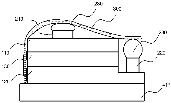
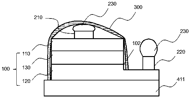
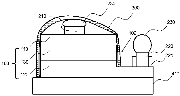
[0057] Hereinafter, the implementation of the present invention will be described in detail with reference to the accompanying drawings and embodiments, so as to fully understand how the present invention applies technical means to solve technical problems and achieve the realization process of technical effects and implement them accordingly. It should be noted that, as long as there is no conflict, each embodiment of the present invention and each feature in each embodiment can be combined with each other, and the technical solutions formed are all within the protection scope of the present invention.

[0058] It should be understood that the terms used in the present invention are only for the purpose of describing specific embodiments, and are not intended to limit the present invention. It is further understood that when the terms "comprising" and "including" are used in the present invention, they are used to indicate the existence of the stated feature, whole, step, and / or ...


PUM


Abstract

The invention discloses a light emitting diode, comprising a semiconductor layer sequence having an active layer between a first conductivity type layer and a second conductivity type layer for generating first light of a first peak wavelength, the first conductivity type layer being located on one side of the positive direction of the semiconductor layer sequence, and the second conductivity typelayer being partially exposed; and a wavelength conversion layer arranged in the positive direction and side wall of the semiconductor layer sequence, the wavelength conversion layer absorbing the first light emitted from the semiconductor layer sequence and emitting second light of a second peak wavelength different from the first peak wavelength; wherein a second electrode and the wavelength conversion layer are on the same side of the light emitting diode, and the distance from the second electrode to the side wall of the semiconductor layer sequence is not less than 50 microns, which solves the problem that the side wall of the semiconductor sequence leaks the first light, and improves the uniformity of light emission of the light emitting diode.

Description

Technical field [0001] The invention belongs to the field of light-emitting semiconductor devices, and specifically relates to a light-emitting diode prepared by wavelength conversion. Background technique [0002] See figure 1 In the conventional LED chip design scheme, the distance between the second electrical connection layer and the sidewall of the semiconductor layer sequence will be maintained at 10-20 μm, so as to reserve as much light-emitting area as possible to improve product brightness. However, under this design, after the core chip is packaged and wired, the fluorescent glue film is easily blocked by the second electrical connection layer when the fluorescent glue film is applied, resulting in insufficient adhesion of the fluorescent glue film and the semiconductor layer sequence. This causes the problem of blue light leakage from the side. Summary of the invention [0003] The present invention proposes a feasible solution to the problem of the background art, and...

Claims


Application Information

Patent Timeline
Patent Type & Authority Applications(China)
IPC IPC(8): H01L33/36H01L33/50H01L33/20H01L33/58H01L33/60
CPCH01L33/20H01L33/36H01L33/502H01L33/58H01L33/60
Inventor 杨力勋蔡琳榕
Owner XIAMEN SANAN OPTOELECTRONICS TECH CO LTD
Why Eureka
Try Eureka