Preparation method of nanoparticle linear array resistor

A nanoparticle and line array technology, applied in the direction of resistance manufacturing, resistors, circuits, etc., can solve the problems of cumbersome operation, complicated process, expensive equipment, etc.

Active Publication Date: 2018-10-12
GUANGZHOU UNIVERSITY
View PDF5 Cites 10 Cited by
  • Summary
  • Abstract
  • Description
  • Claims
  • Application Information

AI Technical Summary

Problems solved by technology

[0003] Common preparation methods for nanoscale resistors include LPNE (Lithographically patterned nanowire electrodeposition) and thin film deposition (thin film depo

Method used


Image

  • Preparation method of nanoparticle linear array resistor
  • Preparation method of nanoparticle linear array resistor
  • Preparation method of nanoparticle linear array resistor

Examples


Embodiment 1

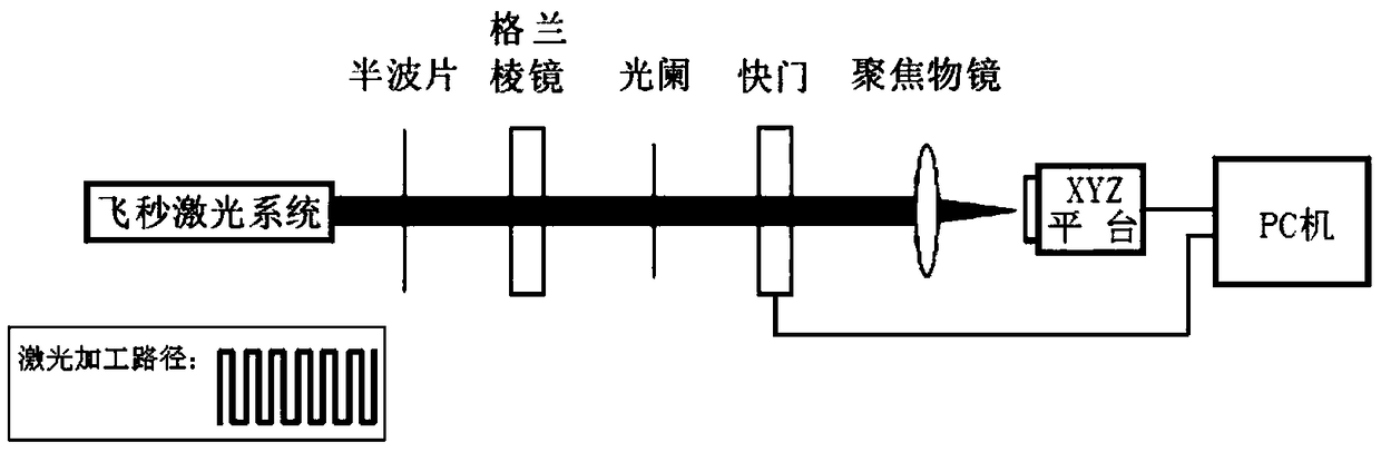
[0024] The invention provides a method for preparing nanoparticle line array resistors, specifically as figure 1 As shown, it includes a femtosecond laser system, a three-dimensional micro-displacement platform, an optical path system, and a PC. The optical path system includes a half-wave plate, a Glan prism, a diaphragm, a shutter, and a focusing objective lens. The prepared sample is placed on the three-dimensional micro-displacement platform through the half-wave plate, Glan prism, diaphragm, shutter and focusing objective lens placed at intervals. The femtosecond pulse laser is focused on the prepared sample through the focusing objective lens, and the three-dimensional micro-displacement platform and the shutter pass through PC control; figure 1 The XYZ platform in is the above-mentioned three-dimensional micro-displacement platform.

[0025] Concrete preparation method comprises the following steps:

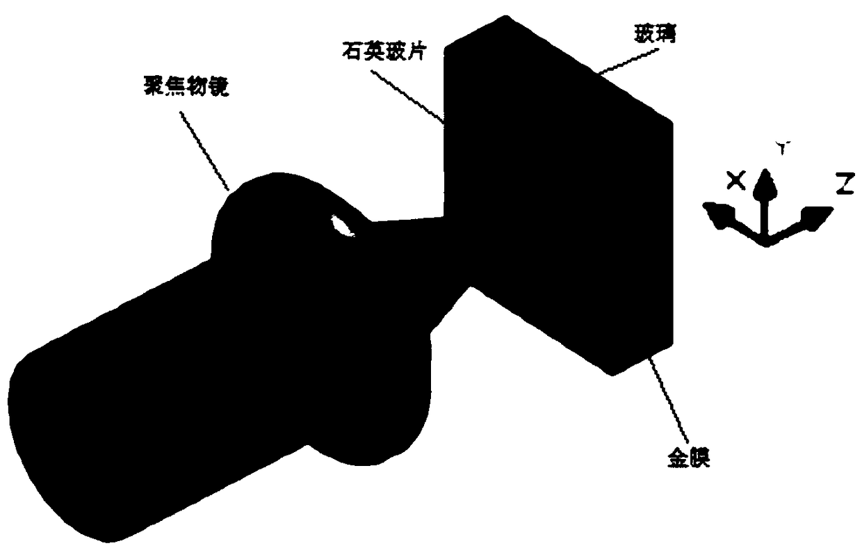
[0026] Step 1. Coating a gold film on the glass surface, and then c...


PUM

PropertyMeasurementUnit
Wavelengthaaaaaaaaaa
Pulse widthaaaaaaaaaa
Focal lengthaaaaaaaaaa

Abstract

The invention provides a preparation method of a nanoparticle linear array resistor. The preparation method comprises the steps: a prepared sample is obtained; the prepared sample is put on a three-dimensional micro displacement platform; femtosecond pulse laser passes through an optical path system to transmit a quartz slide to be focused on the surface of a gold film; a PC controls the three-dimensional micro displacement platform to move in the directions of a Y axis and a Z axis; the gold film is subjected to ablation by the focused laser to form plasma spray in a constraint space; the spayed gold nanoparticles are received by the covered glass, and the gold nanoparticle linear array resistor is obtained on the glass surface; and the morphology features of the gold nanoparticle lineararray resistor are represented. The method is based on a femtosecond laser micro-nano processing platform and is combination with a laser induced backward transfer technology; by controlling femtosecond pulse laser energy density, scanning speed and processing number of branches, the linear array resistor formed by the gold nanoparticles is prepared; and the gold nanoparticle morphology features of different processing parameters are represented by a scanning electron microscope and an atomic force microscope.

Description

technical field [0001] The invention belongs to the rapid preparation technology of composite nanostructure new materials, and is a comprehensive interdisciplinary field of integration of optics, mechanics, electricity, materials and computers, specifically a method for preparing nanoparticle line array resistors. Background technique [0002] Due to the large specific surface area, quantum confinement effect and small size effect of the nanostructure of the material, the nanostructure material has excellent optical, electrical, chemical and mechanical properties different from the bulk material, such as higher surface chemical activity. , gas adsorption advantages, absorption enhancement effect and quantum tunneling effect, etc., are widely used in the field of optoelectronic technology, such as palladium nanometer size resistors can be used to prepare hydrogen sensor devices. [0003] Common preparation methods for nanoscale resistors include LPNE (Lithographically pattern...

Claims


Application Information

Patent Timeline
IPC IPC(8): H01C17/00H01C17/075H01C17/242
CPCH01C17/00H01C17/075H01C17/242
Inventor 张成云刘志宇刘佐濂
Owner GUANGZHOU UNIVERSITY
Why Eureka
Try Eureka