High electron mobility transistor and manufacturing method
A high electron mobility and manufacturing method technology, applied in the field of high electron mobility transistors and manufacturing, can solve the problems of low repeatability, high time consumption, high cost, etc., achieve the effect of reducing impurity defects and improving growth quality
- Summary
- Abstract
- Description
- Claims
- Application Information
AI Technical Summary
Problems solved by technology
Method used
Image
Examples
Embodiment 1
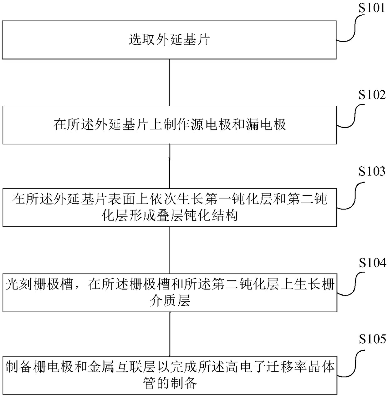
[0028] See figure 1 , figure 1 A schematic flow chart of a method for preparing a high electron mobility transistor provided in an embodiment of the present invention, including:
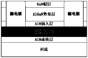
[0029] S101. Select an epitaxial substrate; the epitaxial substrate sequentially includes a substrate, an AlN nucleation layer, a GaN buffer layer, an AlN insertion layer, an AlGaN barrier layer, and a GaN cap layer from bottom to top;
[0030] S102, making a source electrode and a drain electrode on the epitaxial substrate;
[0031] S103, sequentially growing a first passivation layer and a second passivation layer on the surface of the epitaxial substrate to form a stacked passivation structure;
[0032] S104, photoetching a gate groove, growing a gate dielectric layer on the gate groove and the second passivation layer;
[0033] S105 , preparing a gate electrode and a metal interconnection layer to complete the preparation of the high electron mobility transistor.
[0034] Specifically, the f...
Embodiment 2
[0054] Please refer to Figure 2, Figure 2a-2i It is a schematic flow chart of a manufacturing process of a high electron mobility transistor provided by the embodiment of the present invention. This embodiment describes in detail the manufacturing process of the high electron mobility transistor of the present invention on the basis of the first embodiment. include:
[0055] S201, such as Figure 2a As shown, the source and drain electrodes are fabricated on the GaN buffer layer of the epitaxial substrate.
[0056] Among them, the epitaxial substrate can be the initially purchased epitaxial substrate, or it can be the manufactured epitaxial substrate, and the epitaxial substrate includes substrate, nucleation layer, GaN buffer layer, AlN insertion layer, AlGaN potential barrier layer and GaN cap layer.
[0057] Specifically, the substrate is a sapphire substrate.
[0058] S2011, photoetching the source electrode region and the drain electrode region on the GaN cap layer: ...
Embodiment 3
[0138] Further, please refer to image 3 , image 3 The flow chart of another method for manufacturing a high electron mobility transistor provided by the embodiment of the present invention is described in detail in this embodiment on the basis of the first embodiment. Specifically include:
[0139] S301. Select an epitaxial substrate.
[0140] Wherein, the epitaxial substrate sequentially includes a substrate, a nucleation layer, a GaN buffer layer, an AlN insertion layer, an AlGaN barrier layer and a GaN cap layer from bottom to top.
[0141] Specifically, the substrate is a SiC substrate.
[0142] S302 , fabricating a source electrode and a drain electrode on the GaN buffer layer of the epitaxial substrate.
[0143] Wherein, the epitaxial substrate sequentially includes a SiC substrate, a nucleation layer, a GaN buffer layer, an AlN insertion layer, an AlGaN barrier layer and a GaN cap layer from bottom to top.
[0144] S3021, photoetching a source electrode region an...
PUM
| Property | Measurement | Unit |
|---|---|---|
| Thickness | aaaaa | aaaaa |
| Thickness | aaaaa | aaaaa |
| Thickness | aaaaa | aaaaa |
Abstract
Description
Claims
Application Information
 - R&D Engineer
- R&D Manager
- IP Professional
- Industry Leading Data Capabilities
- Powerful AI technology
- Patent DNA Extraction
Browse by: Latest US Patents, China's latest patents, Technical Efficacy Thesaurus, Application Domain, Technology Topic, Popular Technical Reports.
© 2024 PatSnap. All rights reserved.Legal|Privacy policy|Modern Slavery Act Transparency Statement|Sitemap|About US| Contact US: help@patsnap.com


