Display panel and display device

A display panel and substrate technology, applied in the direction of electrical components, electrical solid devices, circuits, etc., can solve the problems of reducing the bending resistance of the display panel, the display brightness and luminous efficiency of the display panel, etc.

Inactive Publication Date: 2018-10-16
EVERDISPLAY OPTRONICS (SHANGHAI) CO LTD
View PDF5 Cites 22 Cited by
  • Summary
  • Abstract
  • Description
  • Claims
  • Application Information

AI Technical Summary

Problems solved by technology

[0004] However, in actual production design, due to technical limitations, the thickness of the current polarizer 14 is usually greater than 100 μm. Undoubtedly, such a thick polarizer 14 will reduce the bending resistance of the display panel.
In addi

Method used


Image

  • Display panel and display device
  • Display panel and display device
  • Display panel and display device

Examples


Embodiment 1

[0032] Embodiment 1 of the present invention provides a display panel. The display panel includes a substrate, an organic light emitting device arranged on the substrate, and a thin film encapsulation layer covering the organic light emitting device. The thin film encapsulation layer includes a plurality of film layers stacked, and the refractive index of each film layer constituting the thin film encapsulation layer increases gradually along the direction approaching the organic light emitting device.

[0033] In actual design, by selecting appropriate materials and thicknesses for making each film layer constituting the thin film encapsulation layer, it can be made that when in use, the external ambient light will be different in the thin film encapsulation layer after it is incident on the film encapsulation layer. The interface of the film layer forms reflected light with a phase difference of 180°, and such reflected light can destructively interfere and cancel each other...

Embodiment 2

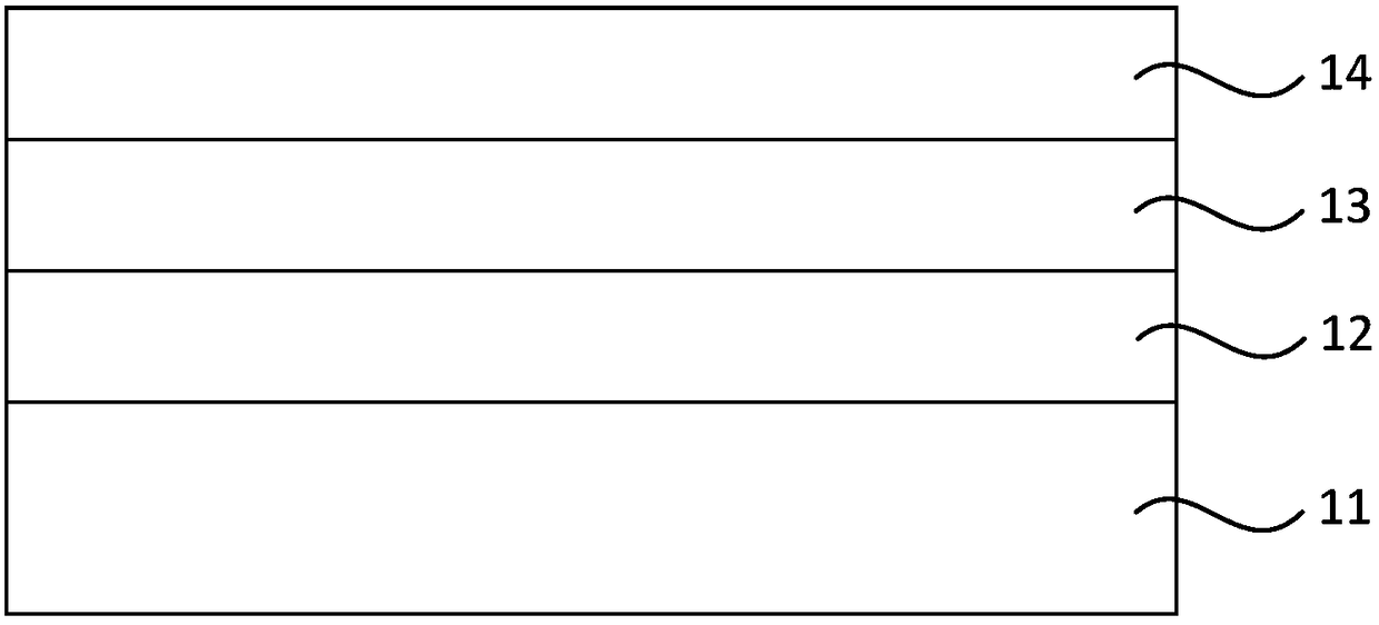
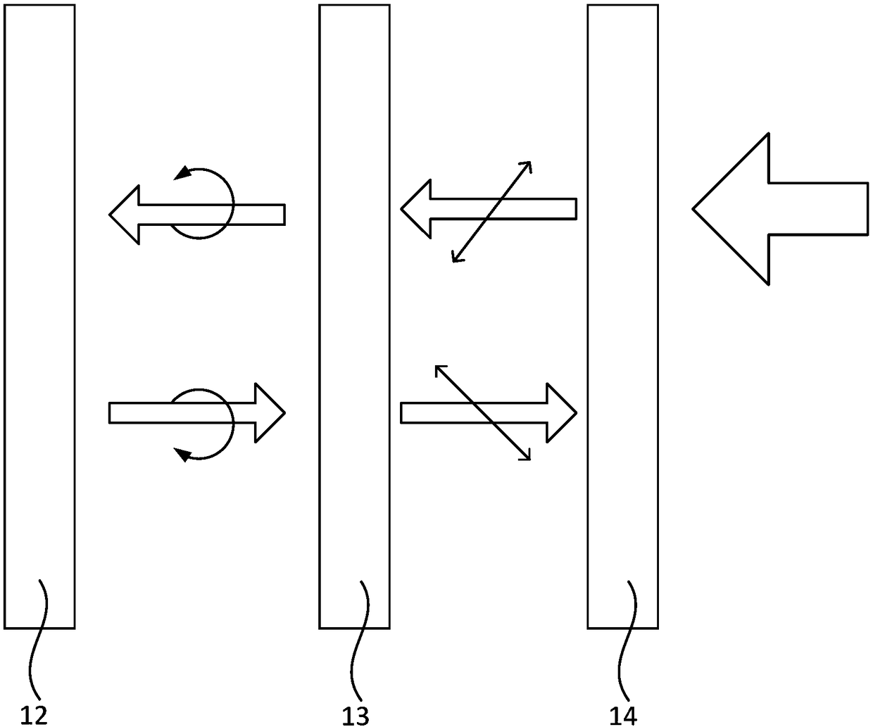
[0038] Figure 2a It is a schematic structural diagram of the display panel provided in Embodiment 2 of the present invention, Figure 2b for Figure 2a Schematic diagram of the working principle of the display panel provided. The technical solution of this embodiment is a specific example of the display panel provided in Embodiment 1. In this embodiment, the thin film encapsulation layer includes three film layers.

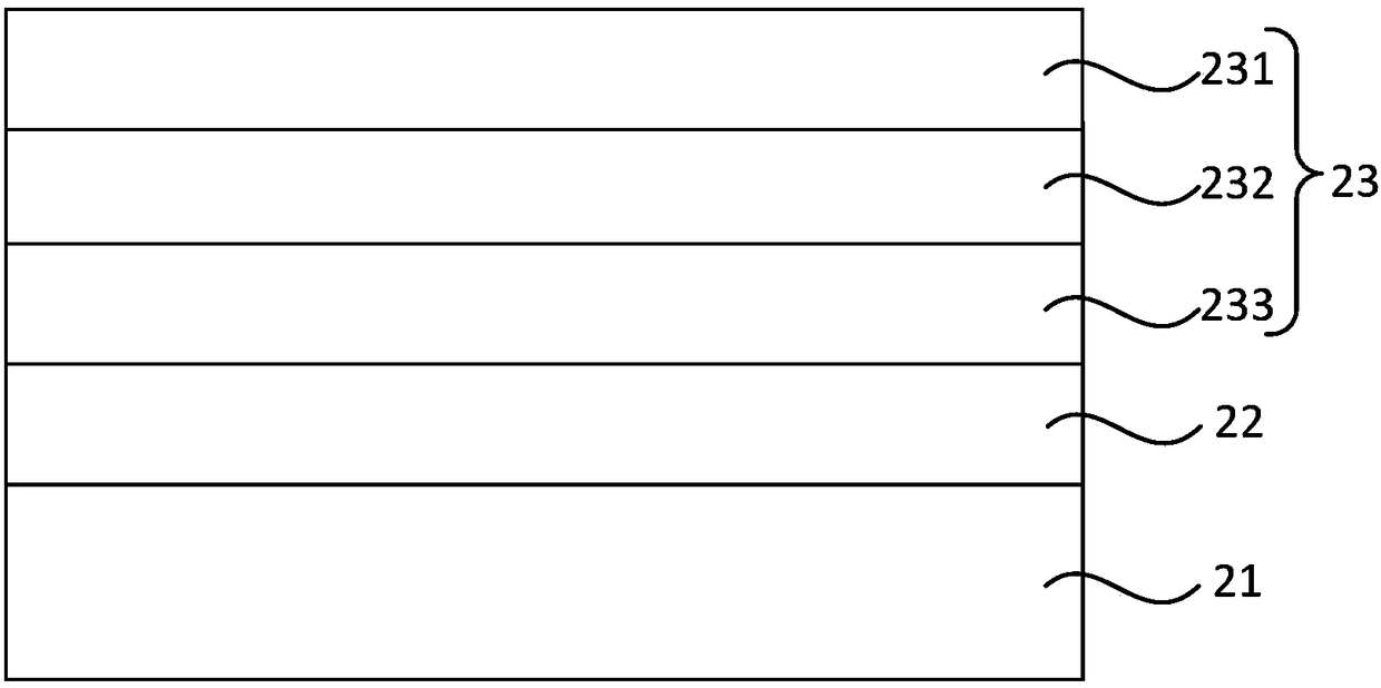
[0039] Specifically, see Figure 2a , the display panel includes a substrate 21, an organic light emitting device 22 disposed on the substrate 21, and a thin film encapsulation layer 23 covering the organic light emitting device 22. The thin film encapsulation layer 23 includes three film layers stacked, and the refractive index of the three film layers constituting the thin film encapsulation layer gradually increases along the direction approaching the organic light emitting device 22 .

[0040] continue to see Figure 2a, the three film layers constitutin...

Embodiment 3

[0045] image 3 It is a schematic structural diagram of a display panel provided by Embodiment 3 of the present invention. Compared with the technical solutions provided by the above embodiments, the display panel provided by the present application further includes a filter film.

[0046] see image 3 , in the display panel, the organic light-emitting device includes pixel light-emitting regions 31 and pixel-defining regions 32 located between the pixel light-emitting regions 31 . The display panel also includes a filter film 26 disposed on the side of the thin film encapsulation layer 23 facing away from the organic light emitting device 22. The filter film 26 includes an opening area 261 and a light-shielding area 262. The opening area 261 corresponds to the pixel light-emitting area 31, and the light-shielding area 262 corresponds to The pixel definition area 32 corresponds. The opening area 261 of the filter film 26 is used to transmit the light emitted by the organic ...


PUM


Abstract

The embodiment of the invention discloses a display panel and a display device. The display panel comprises a substrate, an organic light emitting device disposed on the substrate, and a thin film package layer covering the organic light emitting device; wherein the thin film package layer includes a plurality of film layers stacked in a layer, and the refractive index of the plurality of film layers gradually increases in a direction close to the organic light emitting device. According to the embodiment of the invention, the display panel can solve the problems that the bending resistance ofthe display panel is low, and the display brightness and the luminous efficiency of the display panel are also low since the existing display panel including a polarizer which reduces the thickness of the display panel; and realize the purpose of improving the bending resistance, display brightness and luminous efficiency of the display panel under the premise of ensuring that the display panel has a relatively low reflectivity to external light.

Description

technical field [0001] Embodiments of the present invention relate to display technologies, and in particular, to a display panel and a display device. Background technique [0002] Organic light emitting display (OLED) has become one of the key development directions of the display industry due to its technical advantages such as no need for backlight, high contrast, thin thickness, wide viewing angle, fast response, and good bending resistance. . [0003] In order to improve the contrast and outdoor readability of the display panel, currently the display panel is usually provided with a polarizer to reduce the reflectivity of the display panel to external light. Figure 1a It is a structural schematic diagram of an existing display panel. Figure 1b for Figure 1a The working principle diagram of the display panel. see Figure 1a and Figure 1b , the display panel includes a substrate 11 , an organic light-emitting device 12 , a quarter-wave plate 13 and a polarizer 14 ...

Claims


Application Information

Patent Timeline
IPC IPC(8): H01L27/32H01L51/52
CPCH10K59/12H10K50/8445H10K50/844H10K50/858H10K50/865
Inventor 王历平
Owner EVERDISPLAY OPTRONICS (SHANGHAI) CO LTD
Why Eureka
Try Eureka