
High-temperature packaging method for a wide-band-gap semiconductor silicon carbide power module

A wide-bandgap semiconductor and power module technology, which is applied in semiconductor devices, semiconductor/solid-state device components, electric solid-state devices, etc., can solve problems such as damage to silicon carbide power devices, achieve effective connectivity, improve compression limit, The effect of good high temperature resistance

Active Publication Date: 2018-10-19
江苏芯澄半导体有限公司
View PDF3 Cites 1 Cited by
  • Summary
  • Abstract
  • Description
  • Claims
  • Application Information

AI Technical Summary

Problems solved by technology

[0006] As a result, during the working process, if external force or vibration is received, the silicon carbide power device will directly bear the impact, which may easily cause damage to the silicon carbide power device

Method used


Image

  • High-temperature packaging method for a wide-band-gap semiconductor silicon carbide power module
  • High-temperature packaging method for a wide-band-gap semiconductor silicon carbide power module
  • High-temperature packaging method for a wide-band-gap semiconductor silicon carbide power module

Examples


Embodiment 1

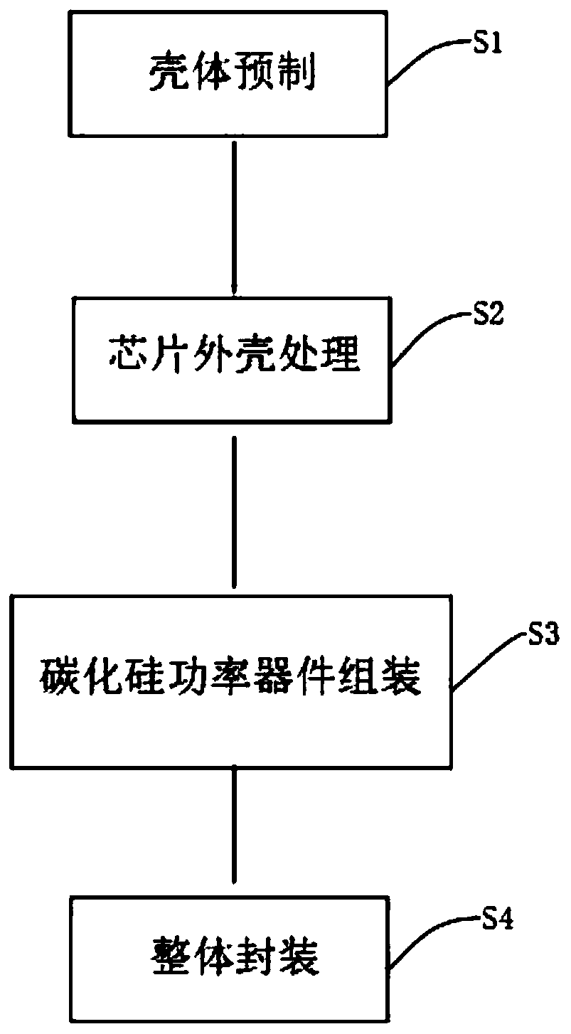
[0033] A high-temperature packaging method for a wide bandgap semiconductor silicon carbide power module, comprising:

[0034] S1: The casing 3 is prefabricated. After the epoxy resin material is prepared, it is put into a mold for finalizing the shape, and the casing 3 is obtained after demoulding. A slot 34 for placing the silicon carbide power device 1 is reserved on the opposite surface of the shell 3 to which the chip belongs, and dibutyl phthalate or dioctyl phthalate is added to the epoxy resin material, and the epoxy The ratio of resin to dibutyl phthalate is 1:0.05~1:0.03, and the ratio of epoxy resin to dioctyl phthalate is 1:0.05~1:0.02;

[0035] S2: Process the chip case 11, open a hole on the case of the silicon carbide power device 1, place an elastic member 13 in the hole, and extend the hole to the inside of the silicon carbide power device 1 to the terminal of the built-in chip to become a wiring hole 16, the wiring hole 16 The side wall is provided with a wi...

Embodiment 2

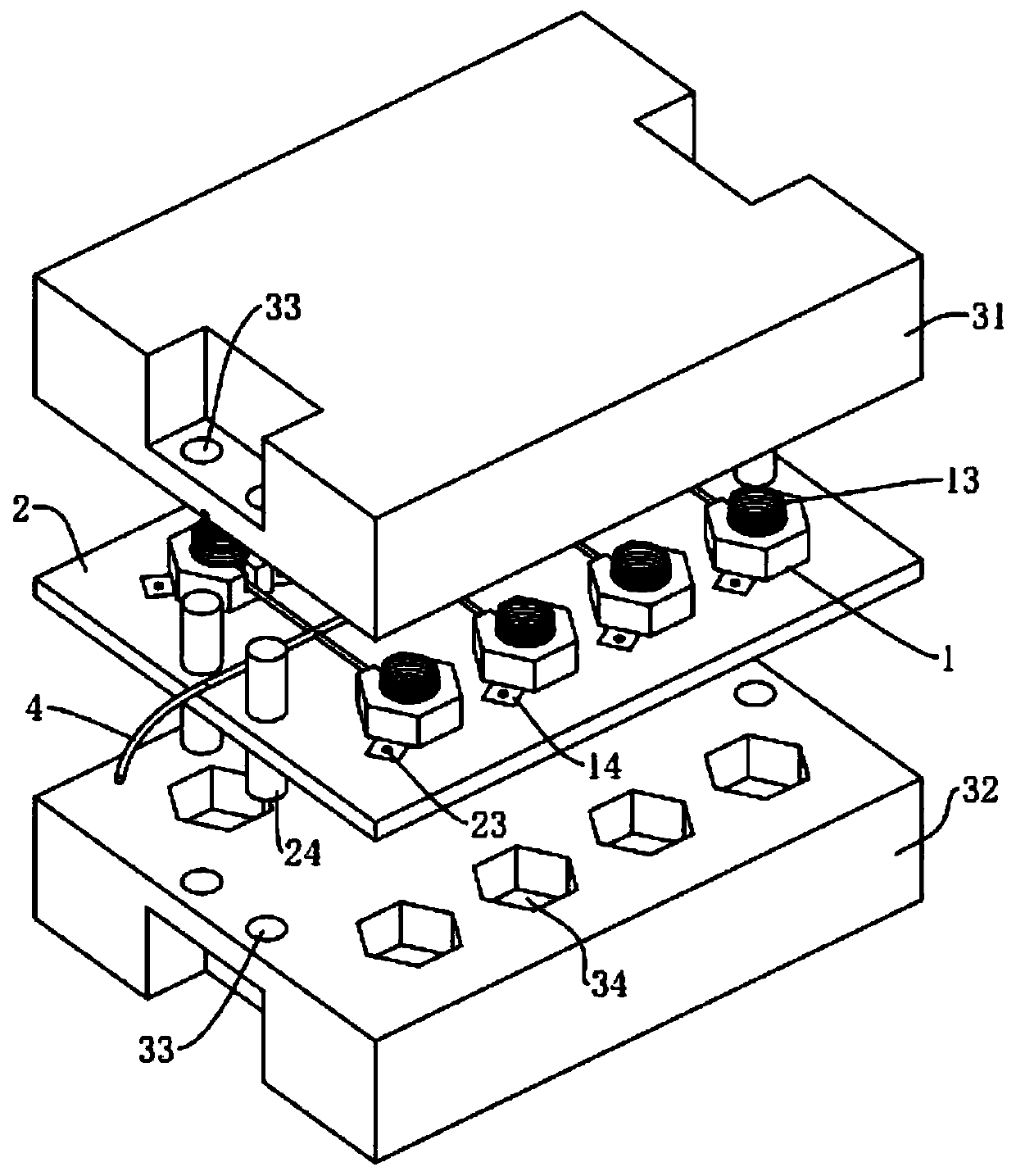
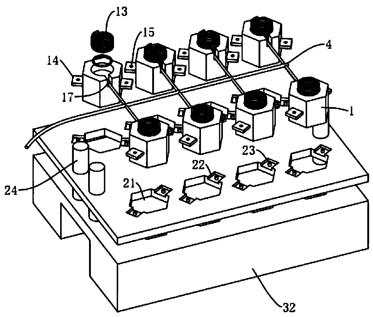
[0039] This embodiment provides a high-temperature packaging structure of a wide-bandgap semiconductor silicon carbide power module using the method of Embodiment 1, as shown in the figure.

[0040] The high-temperature packaging method of a wide bandgap semiconductor silicon carbide power module includes a silicon carbide power device 1 and a wiring group 4 connecting each silicon carbide power device 1, and also includes an isolation liner 2, and the silicon carbide power device 1 is installed on the On the isolation liner 2, and every two silicon carbide power devices 1 form a group, the wiring channels 17 of each group of two silicon carbide power devices 1 are arranged oppositely, and the casing 3 of the silicon carbide power device 1 is provided outside the isolation board , The housing 3 includes an upper housing 31 and a lower housing 32 respectively arranged on two sides of the isolation plate.

[0041] The silicon carbide power device 1 includes a chip casing 11 and ...


PUM


Abstract

The invention discloses a high-temperature packaging method for a wide-band-gap semiconductor silicon carbide power module and relates to the technical field of silicon carbide power module packaging.The high-temperature packaging method comprises the follow steps: S1, modulating an epoxy resin material, placing the epoxy resin material into a mold for shaping, and obtaining a housing after demoulding; S2, opening holes in housings of silicon carbide power devices, and placing elastic members in the holes; S3, mounting the silicon carbide power devices one by one according to mounting positions reserved on an isolation liner plate; S4: making the upper housing and the lower housing draw close to the isolation liner plate, tightening bolts on studs after the housing is buckled, and then completing packaging, wherein the elastic members stay in a compressed state after packaging. According to the scheme of the invention, the silicon carbide power devices are positioned through the prefabricated housing and a buffer is obtained before external force is transmitted to the silicon carbide power devices, so the silicon carbide power devices in the packaged body are better protected.

Description

technical field [0001] The invention relates to the technical field of silicon carbide power module packaging, in particular to a high-temperature packaging method for a wide bandgap semiconductor silicon carbide power module. Background technique [0002] Power semiconductor devices are widely used in computer, network communication, consumer electronics, industrial control, automotive electronics, locomotive traction, steel smelting, high-power power supply, power system and other fields. In addition to ensuring the normal operation of these devices, power devices can also play a role Effective energy saving is indispensable in the development of low-carbon economy, energy conservation and emission reduction, and control of climate warming. [0003] Traditional silicon-based power devices are limited by the inherent physical properties of silicon materials, and have encountered insurmountable difficulties in high-frequency and high-power applications. In this case, power ...

Claims


Application Information

Patent Timeline
Patent Type & Authority Applications(China)
IPC IPC(8): H01L23/02H01L23/08H01L25/11
CPCH01L23/02H01L23/08H01L25/11
Inventor 张浩
Owner 江苏芯澄半导体有限公司
Learn More