Multi-quantum well layer, LED epitaxial structure and preparation method thereof
A multi-quantum well layer and quantum well layer technology, which is applied in the field of InGaN/GaN multi-quantum well layer, LED epitaxial structure and its preparation, and LED epitaxial structure. , Reduce the luminous intensity and other issues, to achieve the effect of not deteriorating the crystal quality, improving the uniformity of the luminous wavelength, and increasing the luminous intensity
- Summary
- Abstract
- Description
- Claims
- Application Information
AI Technical Summary
Problems solved by technology
Method used
Image

Examples
Embodiment 1
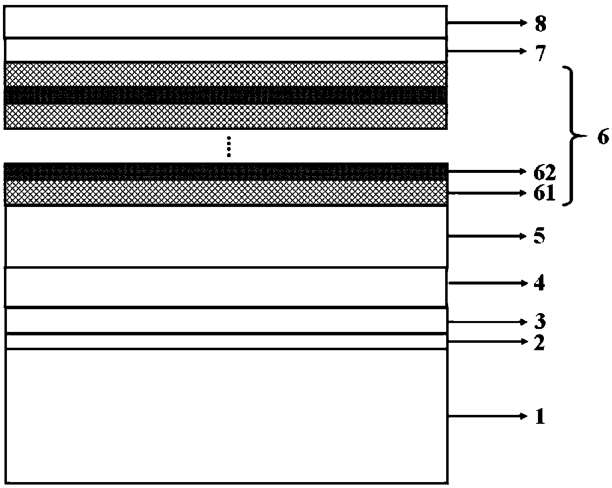
[0076] refer to figure 1 , the present invention provides an InGaN / GaN multi-quantum well layer with graded silicon-doped quantum barriers, the structure is composed of x InGaN quantum well layers and (x+1) GaN quantum barrier layers alternately stacked, x≥1 ; The thickness of the InGaN quantum well layer is 3-5nm; the molar ratio of the In component of the InGaN quantum well layer is 0.1-0.2; the thickness of the GaN quantum barrier layer is 10-15nm; the silicon doping of the first GaN quantum barrier layer The concentration is 5×10 17 -1×10 19 cm -3 , the silicon doping concentration of the second GaN quantum barrier layer is y times the silicon doping concentration of the first GaN quantum barrier layer... The silicon doping concentration of the i-th GaN quantum barrier layer is the first GaN quantum barrier layer layer silicon doping concentration y i-1 times, 0.5<y<1, 1<i≤x, the silicon doping concentration of the (x+1)th GaN quantum barrier layer is 0.
[0077] The...
Embodiment 2
[0094] The characteristics of this embodiment are: step 3) the temperature of the reaction chamber is maintained at 800-1000 ° C, the air pressure is maintained at 200 Torr, and the InGaN / GaN multiple quantum well layer 6 with a gradient silicon-doped quantum barrier is grown, wherein four are grown according to the following sub-steps InGaN quantum well layer and 5 GaN quantum barrier layers; others are the same as in embodiment 1.
Embodiment 3
[0096] The characteristics of this embodiment are: step 3) the temperature of the reaction chamber is kept at 800-1000° C., the air pressure is kept at 200 Torr, and the InGaN / GaN multi-quantum well layer 6 with a gradient silicon-doped quantum barrier is grown, wherein six are grown according to the following sub-steps InGaN quantum well layer and 7 GaN quantum barrier layers; others are the same as embodiment 1.
PUM
| Property | Measurement | Unit |
|---|---|---|
| Thickness | aaaaa | aaaaa |
| Thickness | aaaaa | aaaaa |
| Thickness | aaaaa | aaaaa |
Abstract
Description
Claims
Application Information
 - Generate Ideas
- Intellectual Property
- Life Sciences
- Materials
- Tech Scout
- Unparalleled Data Quality
- Higher Quality Content
- 60% Fewer Hallucinations
Browse by: Latest US Patents, China's latest patents, Technical Efficacy Thesaurus, Application Domain, Technology Topic, Popular Technical Reports.
© 2025 PatSnap. All rights reserved.Legal|Privacy policy|Modern Slavery Act Transparency Statement|Sitemap|About US| Contact US: help@patsnap.com