
LED device with vertical structure, and manufacturing method thereof

A LED device and vertical structure technology, applied in the direction of semiconductor devices, instruments, electrical components, etc., can solve the problems of slow transfer speed, low efficiency, and difficulty in mass production of micro-LED displays, so as to avoid reunion and solve huge Transfer, the effect of facilitating mass transfer

Active Publication Date: 2018-10-19
SHANTOU GOWORLD DISPLAY TECH CO LTD
View PDF3 Cites 2 Cited by
  • Summary
  • Abstract
  • Description
  • Claims
  • Application Information

AI Technical Summary

Problems solved by technology

In the prior art, a large amount of tiny LED devices are transferred and bonded to the base layer of the driving circuit to form an LED array device as the main body of the micro LED display, and a transfer head is generally used to transfer one by one (or multiple batches) of LED devices. However, the transfer speed is slow and the efficiency is low, so it is difficult to realize the mass production of micro-LED displays.

Method used


Image

  • LED device with vertical structure, and manufacturing method thereof
  • LED device with vertical structure, and manufacturing method thereof
  • LED device with vertical structure, and manufacturing method thereof

Examples


Embodiment 1

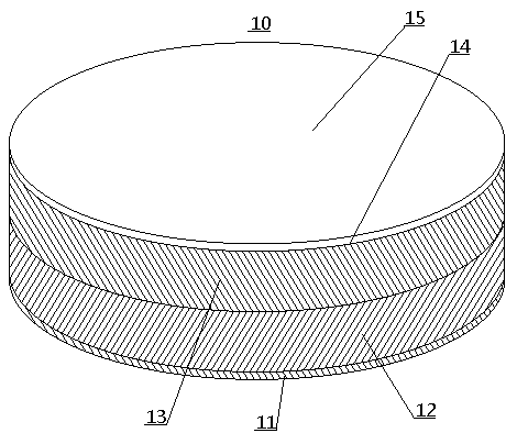
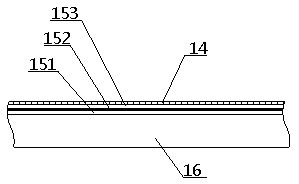
[0039] Such as figure 1 As shown, the LED device 10 is a GaN-based blue light vertical circular LED device with a diameter of 0.3mm (0.03-0.8mm is acceptable), and its film layers are bonding layer 11 and soft magnetic layer from inside to outside. 12. A nonmagnetic metal layer 13, a first electrode 14 and a semiconductor light emitting layer 15. Wherein, the bonding layer 11 is a 5 μm thick tin metal layer (tin alloy layer, indium metal or alloy layer can also be used), the soft magnetic layer 12 is a 40 μm thick iron-nickel alloy layer, and the non-magnetic metal layer 13 is a 40 μm thick copper layer. The metal layer (gold, silver, aluminum metal layer or alloy layer can also be used), the first electrode 14 is a nickel film with a thickness of 100nm; the total thickness of the semiconductor light-emitting layer 15 is 4 μm, which includes an N-type layer (n-GaN) Quantum wells (MQWs) 152 and a p-type layer (p-GaN) 153 as the second electrode of the LED device.

[0040] The...


PUM


Abstract

Provided is an LED device with a vertical structure, comprising a semiconductor light-emitting layer, and a first electrode and a second electrode, which are respectively arranged in the inner side and the outer side of the light-emitting layer. A soft magnetic layer composed of soft magnetic metal is arranged on the first electrode. When the LED device is used for manufacturing a micro LED display, the LED device can be transferred to a driving circuit base layer in a faster and the highly-efficient manner with giant quantity so as to form an LED array device. In addition, the invention further provides a manufacturing method of the LED device.

Description

technical field [0001] The present invention relates to an LED device, especially a vertical structure LED device, and also relates to a manufacturing method of the LED device. Background technique [0002] A micro-LED display such as micro-LED or mini-LED is generally a display formed by transferring and bonding a large number of tiny LEDs (light-emitting diodes) to a base layer of a driving circuit. In the prior art, a large amount of tiny LED devices are transferred and bonded to the base layer of the driving circuit to form an LED array device as the main body of the micro LED display, and a transfer head is generally used to transfer one by one (or multiple batches) of LED devices. However, the transfer speed is slow and the efficiency is low, so it is difficult to realize the mass production of micro-LED displays. [0003] Therefore, in the manufacture of micro-LED displays, how to more efficiently transfer and bond a huge amount of tiny LED devices to the base layer ...

Claims


Application Information

Patent Timeline
Patent Type & Authority Applications(China)
IPC IPC(8): H01L33/36H01L33/00
CPCG09F9/33H01L33/005H01L33/0062H01L33/0075H01L33/32H01L33/36H01L33/44
Inventor 沈奕吕岳敏
Owner SHANTOU GOWORLD DISPLAY TECH CO LTD
Learn More