Fabrication method of thin film micro-optical structure based on photolithography and chemical mechanical polishing

A chemical-mechanical and micro-optical technology, applied in the field of photolithography and chemical-mechanical polishing, to achieve the effects of reducing effective mode volume, avoiding loss, and controlling mode dispersion

Active Publication Date: 2018-10-26
SHANGHAI INST OF OPTICS & FINE MECHANICS CHINESE ACAD OF SCI
View PDF4 Cites 13 Cited by
  • Summary
  • Abstract
  • Description
  • Claims
  • Application Information

AI Technical Summary

Problems solved by technology

However, traditional chemical mechanical polishing is used to prepare flat material surfaces, rather than to improve the overall quality of on-chip thin film structures.

Method used


Image

  • Fabrication method of thin film micro-optical structure based on photolithography and chemical mechanical polishing
  • Fabrication method of thin film micro-optical structure based on photolithography and chemical mechanical polishing

Examples


Embodiment Construction

[0031] The present invention will be further described below by examples and accompanying drawings, but the protection scope of the present invention should not be limited by this.

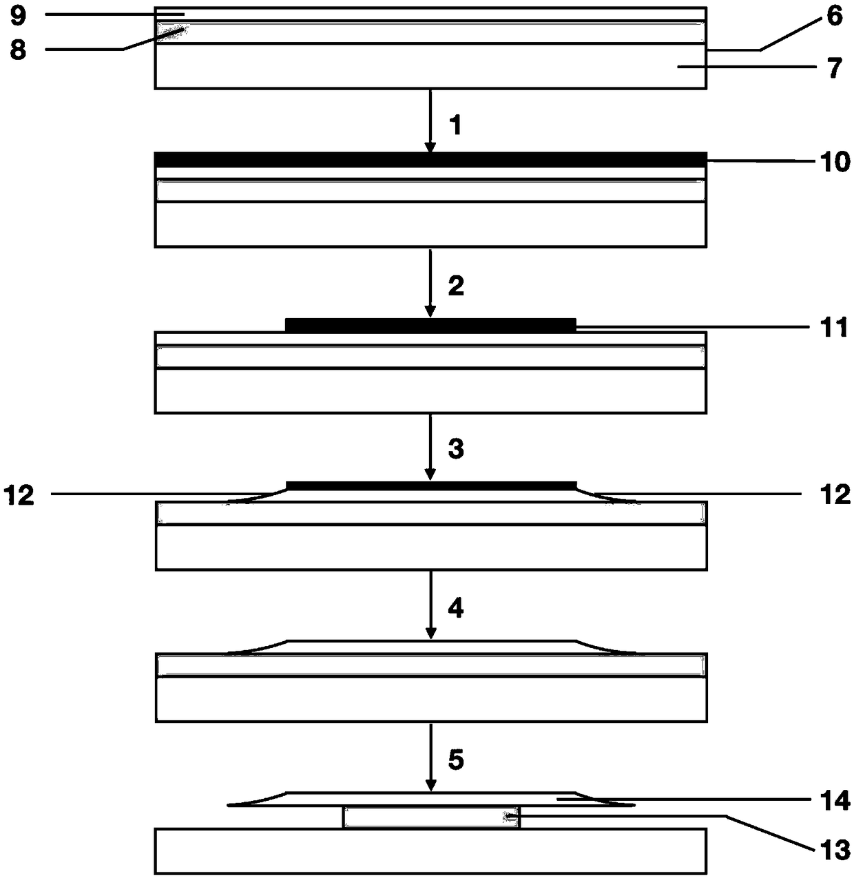
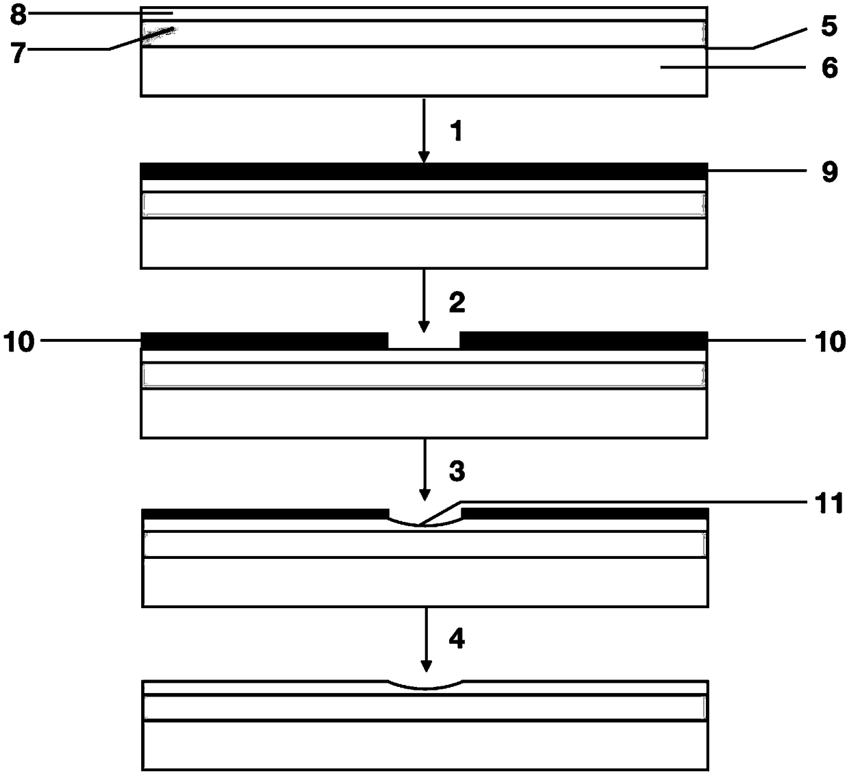
[0032] see first figure 1 , figure 1 It is a schematic flow chart of the method for preparing an optical whispering gallery mode microcavity on a chip by using photolithography technology combined with chemical mechanical polishing. Now, the method of the present invention is illustrated by taking the lithium niobate single crystal thin film on a chip as an example. As can be seen from the figure, the present invention utilizes photolithography The method for preparing an on-chip optical whispering gallery mode microcavity combined with chemical mechanical polishing includes the following five steps:

[0033] (1) Plating Cr metal film on the surface: Take an on-chip single crystal lithium niobate film sample 6 with a size of 3mm×4mm×1mm, which is made of a substrate 7 with a thickness of about 1m...


PUM


Abstract

The invention discloses a fabrication method of a thin film micro-optical structure based on photolithography and chemical mechanical polishing. The fabrication method comprises the steps of plating of a metal layer on a thin film surface, selective removal of a metal film by photolithography, chemical mechanical polishing and chemical etching. An on-chip micro-optical device fabricated by the method disclosed by the invention has extremely high surface finish and very low optical loss. The method is suitable for fabricating high-quality micro-optical structures (including but not limited to micro-disk cavities, micro-ring cavities, optical waveguides and couplers) on various on-chip films (including but not limited to lithium niobate single crystal films, quartz films, silicon films, silicon dioxide films, diamond films and the like).

Description

technical field [0001] The invention relates to photolithography technology and chemical mechanical polishing, in particular to a method for preparing on-chip microstructures (including microcavity discs, microrings, optical waveguides and their integrated structures) by using photolithography technology combined with chemical mechanical polishing. This method is applicable to various on-chip thin film materials, including but not limited to lithium niobate single crystal thin film, quartz thin film, silicon thin film, silicon dioxide thin film, diamond thin film and the like. Background technique [0002] Micro-optical devices refer to micro-structured optical devices with a structure size above the submicron level and a surface roughness up to the nanometer level. On-chip micro-optical devices generally significantly increase the interaction between light and matter by localizing the light field in space and even in time. In basic research and engineering applications, suc...

Claims


Application Information

Patent Timeline
Patent Type & Authority Applications(China)
IPC IPC(8): G03F7/20B24B37/10B24B37/04
CPCB24B37/042B24B37/10G03F7/70216
Inventor 程亚张健皓伍荣波乔玲玲林锦添
Owner SHANGHAI INST OF OPTICS & FINE MECHANICS CHINESE ACAD OF SCI
Why Eureka
Try Eureka