

Package structure
A technology of packaging structure and packaging layer, which is applied to semiconductor/solid-state device parts, semiconductor devices, electrical components, etc., can solve the problems of increasing the volume of the packaging structure, unable to meet the design requirements of miniaturization, and increasing the number of circuit layers, etc. To achieve the effect of reducing the degree of impact
- Summary
- Abstract
- Description
- Claims
- Application Information
AI Technical Summary
Problems solved by technology
Method used
Image

Examples
Embodiment Construction
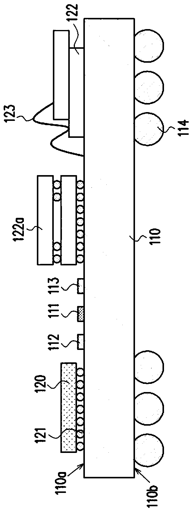
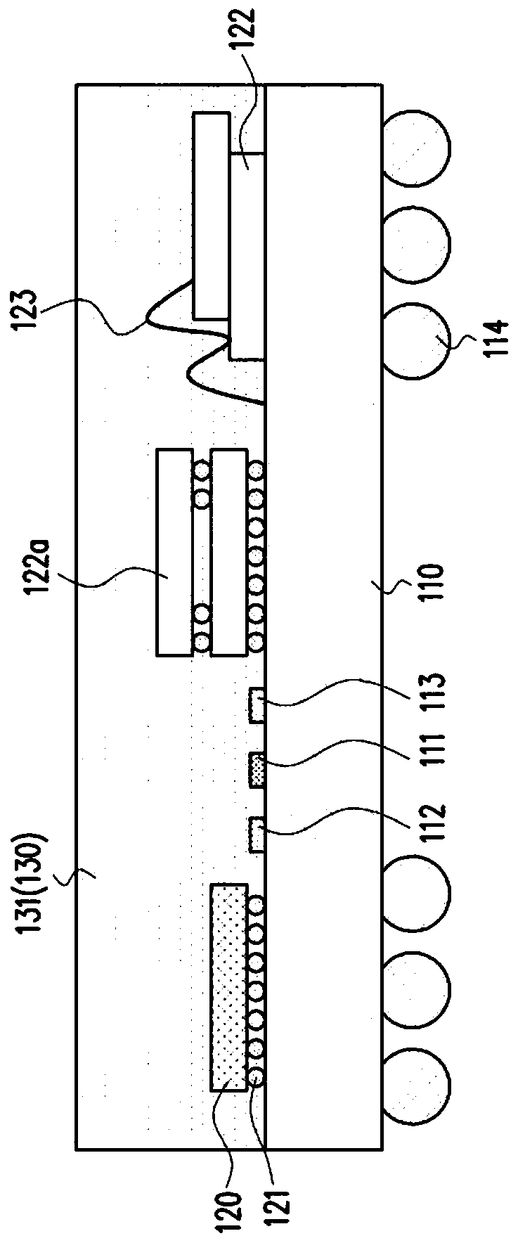
[0050] Figure 1A , Figure 1B , Figure 1D , Figure 1F to Figure 1I is a schematic cross-sectional view of the manufacturing process of the packaging structure according to the first embodiment of the present invention. First, please refer to Figure 1A , providing a circuit carrier 110 provided with a first chip 120 and a second chip 122, 122a, wherein the circuit carrier 110 has a first surface 110a and a second surface 110b opposite to the first surface 110a, and the circuit carrier 110 It includes a first pad 111 and a second pad 112 . The first pads 111 and the second pads 112 are located on the first surface 110 a of the circuit carrier 110 , and the shape, size or quantity of the first pads 111 or the second pads 112 are not limited. For example, the shape of the first pad 111 or the second pad 112 can be a strip shape, a disk shape or a square disk shape. In this embodiment, the first pad 111 may be a ground pad, and the second pad 112 may be electrically connect...
PUM
 Abstract
Description
Claims
Application Information