
A semiconductor diode forming system

A diode and semiconductor technology, applied in the field of semiconductor diode molding systems, can solve the problems of the sharpness of the molding knife edge not being improved, the diode cannot be pre-clamped, the diode cannot be pre-cut, etc., so as to improve the shearing effect and the clamping effect. , the effect of improving efficiency

Active Publication Date: 2020-09-04
江苏芯格诺电子科技有限公司
View PDF8 Cites 0 Cited by
  • Summary
  • Abstract
  • Description
  • Claims
  • Application Information

AI Technical Summary

Problems solved by technology

However, this technical solution cannot be aimed at diodes of different sizes and the diode cannot be pre-clamped during the clamping of the diode; at the same time, the diode cannot be pre-cut during the shearing process of the diode, and the sharp edge of the forming knife has not been improved.
Therefore, the technical solution is limited

Method used


Image

  • A semiconductor diode forming system
  • A semiconductor diode forming system
  • A semiconductor diode forming system

Examples


Embodiment approach

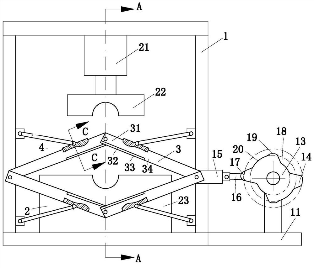
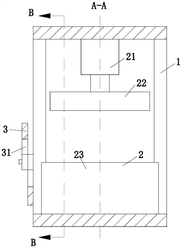
[0025] As an embodiment of the present invention, the outer ring of the No. 1 rotating wheel 13 is composed of two symmetrical No. 1 arcs 14, two symmetrical No. 2 arcs 18, two symmetrical No. 3 arcs 19 and two symmetrical The No. 4 arc 20 is formed; one side of the No. 3 arc 19 is adjacent to the No. 2 arc 18, and the other side of the No. 3 arc 19 is adjacent to the No. 4 arc 20; the No. 1 arc 14 is in the No. 2 arc Between the arc 18 and the fourth arc 20; the No. 1 rotating wheel 13 is provided with a No. 2 chute on the side, and the No. 2 slider 17 slides in the No. 2 chute; the No. 2 slider 17 is on the second The motion trajectory in the No. 2 chute produces different effects; first, when the No. 2 slider 17 is in the No. 1 arc position 14, the No. 2 plate 31 is fully opened at this time, and the forming knife 32 in the No. The diode does not have a shearing effect. When the No. 2 slider 17 moves to the position of the No. 2 arc 18, the No. 2 plate 31 is slowly closed, ...


PUM


Abstract

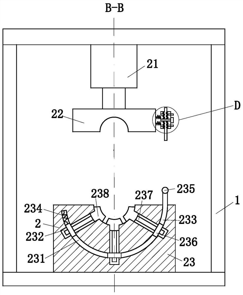
The invention belongs to the technical field of production of semiconductor diodes, and particularly relates to a semiconductor diode forming system. The forming system comprises a rack, a first plate, a clamping module, a shearing module, a cutter grinding block and a position control unit; a fixed bolt is unscrewed, up and down moving is carried out, a fourth plate is moved to the proper position, the fixed bolt is screwed again, the extension length of the fourth plate is changed, the rotation amplitude of an annular rack is adjusted, the rotation amplitude of the annular rack is changed, correspondingly, the sliding distance of an annular block in a fourth sliding groove is changed, semiconductor diode leads with different thicknesses can be clamped, through the motion track of a second sliding block in a first rotation wheel, a forming knife in a second plate carries out pre-shearing, expanding and shearing on the semiconductor diode leads, the cutter grinding block carries out cutter grinding on a forming knife, and therefore a cutting edge of the forming knife is sharp, and the shearing efficiency and effect of the semiconductor diode leads can be improved.

Description

technical field [0001] The invention belongs to the technical field of semiconductor diode production, in particular to a semiconductor diode forming system. Background technique [0002] Diodes, also known as crystal diodes, are referred to as diodes. In addition, there are early vacuum electronic diodes; it is an electronic component with unidirectional conduction current. In electronic components, a device with two electrodes that allows current to flow in only one direction. The most common function of diodes is to allow current to pass in only one direction (called forward bias) and block when reversed (called reverse bias). Therefore, diodes can be thought of as electronic versions of check valves. [0003] There are also some technical solutions for diode forming devices in the prior art. For example, a Chinese patent with the application number of 201120381398.X discloses a diode forming device in the field of semiconductor diodes, including a base, a U-shaped slot...

Claims


Application Information

Patent Timeline
Patent Type & Authority Patents(China)
IPC IPC(8): H01L21/687B28D5/04B28D7/04B28D7/00B24B3/36
CPCB24B3/368B28D5/0058B28D5/0082B28D5/04
Inventor 陈欣洁张家俊
Owner 江苏芯格诺电子科技有限公司
Learn More