Terahertz broadband absorber based on doped semiconductor with coating film

A semiconductor and terahertz technology, applied in the field of terahertz broadband absorbers, can solve the problems of size and bandwidth process complexity that are difficult to achieve a good balance, and there are few terahertz broadband absorbers, and achieve near-perfect anti-reflection and strong The effect of absorbing properties

Active Publication Date: 2018-11-06
SOUTH CHINA NORMAL UNIVERSITY
View PDF4 Cites 2 Cited by
  • Summary
  • Abstract
  • Description
  • Claims
  • Application Information

AI Technical Summary

Problems solved by technology

There are relatively few studies on terahertz broadband absorbers, and the design methods of broadband absorbers that have been proposed so far are difficult to achieve a good balance in terms of size, bandwidth, and process complexity

Method used


Image

  • Terahertz broadband absorber based on doped semiconductor with coating film
  • Terahertz broadband absorber based on doped semiconductor with coating film
  • Terahertz broadband absorber based on doped semiconductor with coating film

Examples


Embodiment 1

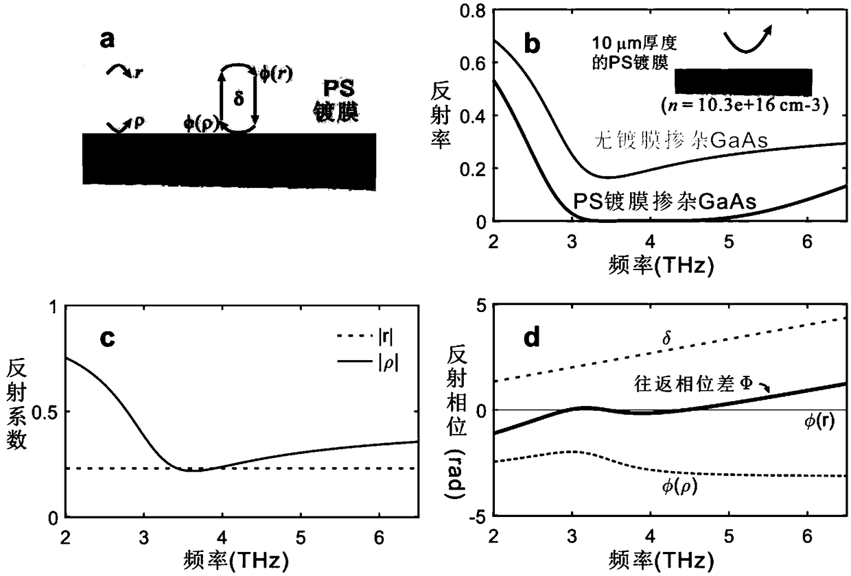
[0045] For the terahertz broadband absorber based on coating doped semiconductor of this embodiment, please refer to image 3(a) includes doped GaAs and PS (Polystyrene) coating, and the PS coating is arranged above the doped GaAs.

[0046] In the present embodiment, each parameter of doping GaAs is: ε GaAs =12.9+7.9×10 -28 ω 2 ;m * =0.079m 0 , m 0 is the free electron mass; τ=μm * / e, μ is the DC electron mobility, and μ changes with the carrier concentration n; n=10.3×10 16 cm -3 (mobility μ = 4000cm 2 V -1 the s -1 , n-type doping); the thickness is 300 μm.

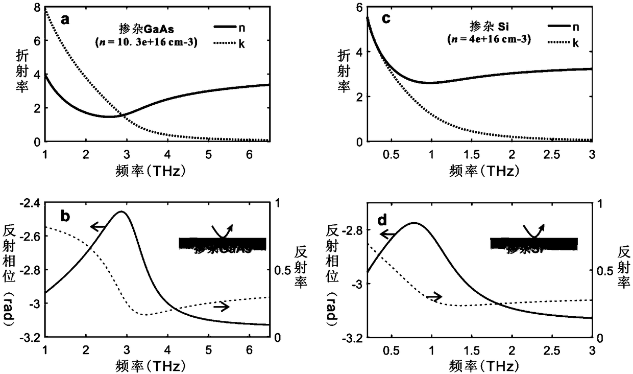
[0047] see figure 2 (a), which is the refractive index dispersion curve of the doped GaAs of the present embodiment (wherein, n represents the real part, and k represents the imaginary part), it can be seen that the refractive index of the doped GaAs is shown as Drude dispersion, and a certain In the wavelength band, the condition of anomalous reflection phase dispersion is satisfied. see figure 2 (b),...

Embodiment 2

[0051] The frequency range of broadband absorption can be adjusted by changing the doping concentration of the semiconductor and the coating thickness. Changing the doping concentration of the semiconductor will change its refractive index, and at the same time, the reflection phase, reflection coefficient, and frequency range of the abnormal dispersion of the reflection phase will also change accordingly. Coatings with different thicknesses are designed to compensate for the reflection phase of doped semiconductors. Anomalous dispersion, so that the corresponding broadband anti-reflection can be realized.

[0052] The terahertz broadband absorber based on coating doped semiconductor in this embodiment is basically the same as that in Embodiment 1, except that the doping concentration of doped GaAs and the thickness of the PS coating are different.

[0053] Figure 4 (a) shows the doping concentration of doped GaAs was 3.1×10 16 cm -3 (μ=5500cm 2 V -1 the s -1 , n-type d...

Embodiment 3

[0055] For the terahertz broadband absorber based on coating doped semiconductor of this embodiment, please refer to Figure 5 (a) includes doped Si and PE (Polyethylene) coating, and the PE coating is arranged on the doped Si.

[0056] In the present embodiment, each parameter of doping Si is: ε Si =(3.415) 2 ; m * =0.26m 0 , m 0 is the mass of free electrons; doping concentration n=4×10 16 cm -3 (mobility μ = 4000cm 2 V -1 the s -1 , n-type doping); the thickness is 300 μm.

[0057] see figure 2 (c), which is the refractive index dispersion curve of the doped Si of the present embodiment (wherein, n represents the real part, and k represents the imaginary part), it can be seen that the refractive index of the doped Si is shown as Drude dispersion, and a certain In the wavelength band, the condition of anomalous reflection phase dispersion is satisfied. see figure 2 (d), which shows the reflectance and reflection phase of the terahertz wave from the air to the ...


PUM


Abstract

The present invention relates to a Terahertz broadband absorber based on a doped semiconductor with a coating film. The Terahertz broadband absorber comprises a doped semiconductor layer and a coatingfilm layer, the coating film layer is arranged at the upper portion of the doped semiconductor layer, the doped semiconductor has high absorption features at the Terahertz waveband and has a refractive index showing Drude dispersion, and the reflection phase of the doped semiconductor has anomalous dispersion at some frequencies of the Terahertz, namely, the reflection phase is reduced with the increasing of the frequency. The Terahertz broadband absorber employs the anomalous dispersion of the doped semiconductor in the Terahertz waveband reflection phase to perform coating film on the dopedsemiconductor to allow the anomalous dispersion of the doped semiconductor reflection phase to be mutually offset with the normal dispersion of a propagation phase in the coating film and meet the absent reflection phase condition in a wide frequency range so as to achieve Terahertz broadband absent reflection and approximate perfect absorption. Besides, the doping concentration and the coating film thickness are changed to regulate the frequency range of generation of the broadband absent reflection and the approximate perfect absorption.

Description

technical field [0001] The invention relates to the technical field of electromagnetic functional materials, in particular to a terahertz broadband absorber based on coating doped semiconductors. Background technique [0002] Terahertz waves refer to electromagnetic waves with a frequency in the range of 0.1THz to 10THz. Because of their unique properties, they have irreplaceable application value in security imaging, short-distance high-speed communication and other fields. Terahertz absorber, as an important electromagnetic wave device, is closely related to the development of terahertz wave detection, communication and imaging systems. [0003] The design principles of terahertz absorbers are divided into two categories: narrowband and broadband. Terahertz narrow-band absorbers have achieved satisfactory absorption performance under the principle of anti-reflection and metamaterial impedance matching, and are currently developing further in the direction of size reductio...

Claims


Application Information

Patent Timeline
Patent Type & Authority Applications(China)
IPC IPC(8): G02B5/00
CPCG02B5/003
Inventor 石风华陈溢杭
Owner SOUTH CHINA NORMAL UNIVERSITY
Why Eureka
Try Eureka