A kind of deposition method of microcrystalline silicon thin film

A technology of microcrystalline silicon thin film and deposition method, which is applied in chemical instruments and methods, single crystal growth, crystal growth, etc., can solve the problems of low photoelectric conversion efficiency, lower manufacturing cost, and low growth rate, and achieve large-area low-temperature Preparation, strong absorption properties, uniform grain effect

Inactive Publication Date: 2011-12-28
INST OF METAL RESEARCH - CHINESE ACAD OF SCI
View PDF0 Cites 2 Cited by
  • Summary
  • Abstract
  • Description
  • Claims
  • Application Information

AI Technical Summary

Problems solved by technology

The problem with this method of preparing microcrystalline silicon thin films is that the growth rate is low Not conducive to reducing manufacturing costs
[0008] The above-mentioned preparation of microcrystalline silicon thin films by direct deposition method has the following problems to varying degrees: low growth rate, which is not conducive to reducing manufacturing costs; low crystallinity, about 50%; low mobility, low photoelectric conversion efficiency

Method used


Image

  • A kind of deposition method of microcrystalline silicon thin film
  • A kind of deposition method of microcrystalline silicon thin film
  • A kind of deposition method of microcrystalline silicon thin film

Examples


Embodiment 1

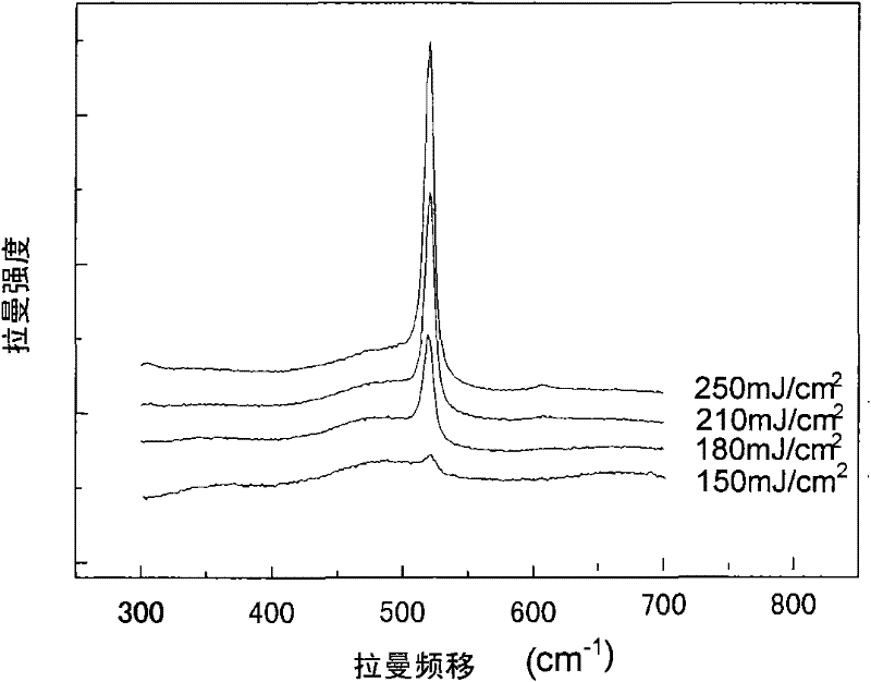
[0026] A 1.7 μm thick amorphous silicon film was deposited on glass by plasma enhanced chemical vapor deposition (PECVD). The discharge gas is Ar, the reaction gas is SiH 4 . The deposition process parameters are: the background vacuum of the deposition chamber is 7×10 -3 Pa, SiH 4 The flow rate is 10sccm, the Ar flow rate is 70sccm, the deposition temperature is ~300°C, the pressure in the reaction chamber is 3.0Pa, the microwave power is 600W, and the deposition time is 6h.

[0027] The pre-deposited a-Si film was cleaned successively with acetone and alcohol solution, dried and fixed on the sample stage, ready for laser surface crystallization. The excimer laser is used as the laser source, the laser is filled with working gas KrF, and the pressure is maintained at 0.5MPa, and argon is introduced as the protective gas of the workpiece, and the pump pulse is gradually adjusted. When the pump pulse with a peak value of 12-20kV is applied to between the discharge electrode...

Embodiment 2

[0033] The difference from Example 1 is:

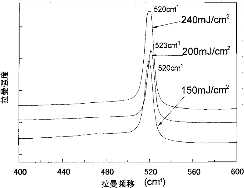
[0034] A 700nm thick amorphous silicon film was deposited on glass by plasma enhanced chemical vapor deposition (PECVD). The discharge gas is Ar, the reaction gas is SiH 4 . The deposition process parameters are: the background vacuum of the deposition chamber is 7×10 -3 Pa, SiH 4 The flow rate is 10sccm, the Ar flow rate is 70sccm, the deposition temperature is ~300°C, the pressure in the reaction chamber is 3.0Pa, the microwave power is 600W, and the deposition time is 4h.

[0035] The pre-deposited a-Si film was cleaned successively with acetone and alcohol solution, dried and fixed on the sample stage, ready for laser surface crystallization. The excimer laser is used as the laser source, the laser is filled with the working gas ArF, and the pressure is maintained at 0.5MPa, and the argon gas is introduced as the protective gas of the workpiece, and the pump pulse is gradually adjusted. When the pump pulse with a peak value of...


PUM

PropertyMeasurementUnit
laser pulse widthaaaaaaaaaa
thicknessaaaaaaaaaa
particle sizeaaaaaaaaaa

Abstract

The invention belongs to the field of semiconductor materials, and relates to a method for preparing a microcrystalline silicon thin film. Specifically, it is a method of preparing a thin layer of microcrystalline silicon layer on the surface of an amorphous silicon film deposited on a glass substrate by laser surface crystallization. The amorphous silicon film deposited directly on the glass plate is partially transformed into microcrystalline silicon by laser heating and crystallization; the laser heating crystallization method is to place the sample of the amorphous silicon film on a laser On the sample stage, the laser beam is irradiated, the amorphous silicon film absorbs the energy of the laser and converts it into its own energy, local melting and recrystallization occur, and the surface crystallization process makes the amorphous silicon transform into microcrystalline silicon. The invention can solve the problems of low growth rate, low crystallinity, low mobility and low photoelectric conversion efficiency in the prior art, and the microcrystalline silicon film crystallized by excimer laser has high crystallinity, uniform crystal grains, and Realize the advantages of large-area low-temperature preparation and short process cycle.

Description

Technical field: [0001] The invention belongs to the field of semiconductor materials, and relates to a method for preparing a microcrystalline silicon thin film. Specifically, it is a method for preparing a thin microcrystalline silicon (μc-Si) layer on the surface of an amorphous silicon (a-Si) thin film deposited on a glass substrate by laser surface crystallization. Background technique: [0002] As the second generation of solar cells, silicon thin-film solar cells have been widely used in industrial production due to their advantages such as sufficient raw materials, low composition, low energy consumption, and easy large-scale production. Silicon thin films mainly include amorphous silicon, microcrystalline silicon and polycrystalline silicon thin films. Among them, microcrystalline silicon thin film is a mixed-phase disordered semiconductor material between amorphous silicon and single crystal silicon, which has both the stable optical properties of single crystal s...

Claims


Application Information

Patent Timeline
Patent Type & Authority Applications(China)
IPC IPC(8): C30B29/06C30B1/02
Inventor 肖金泉赵彦辉崔连武华伟刚宫骏孙超黄荣芳
Owner INST OF METAL RESEARCH - CHINESE ACAD OF SCI
Why Eureka
Try Eureka