Microfluidic chip

a microfluidic chip and microfluidic technology, applied in the field of microfluidic chips, can solve the problems of increasing production costs, unsatisfactory chip quality, and high equipment requirements for this process, and achieve the effects of reducing production costs, ensuring quick reaction to temperature variations, and large surface area

Inactive Publication Date: 2006-08-24
IND TECH RES INST
View PDF0 Cites 18 Cited by
  • Summary
  • Abstract
  • Description
  • Claims
  • Application Information

AI Technical Summary

Benefits of technology

[0017] Therefore, to achieve the above-mentioned objective, the invention provides a microfluidic chip, which can be utilized in the biochemical reaction process required such that the localized temperature control of the microchannel is achieved for controlling the temperature of the biochemical cultivation fluid utilized in the cell cultivation. In this connection, the microfluidic chip is mainly composed of a main body made of transparent material and an electrode layer, wherein the microchannel is provided in the main body, so that the test fluid can be made to flow in the microchannel of the main body while the electrode layer is provided with the heater wire and the sensor wire disposed on one side and in the vicinity of the microchannel respectively, thus supplying heat energy to the test fluid contained therein and measuring its temperature, as such fully taking advantage of its large surface area, and ensuring quick reaction to the temperature variations of the heat source, thus achieving the rapid rise and fall of the temperature of the microfluidic chip, and realizing the purpose of multiplying the sample body in a very short time. In addition, through the application of the invention, the temperature control process can be achieved without utilizing the insulation layer, so that the production cost can be reduced significantly, meanwhile, the precise temperature control of the microfluidic chip can also be realized.

Problems solved by technology

The bonded glass substrate and silicon substrate thus produced has the characteristics of single side transmittance of light, however, the equipment required to use in this process is quite expensive, thus raising the production cost.
However, the quality of the chip thus produced is not quite satisfactory, since the adhesive material is liable to block the micro-channel in the substrate.
Besides, the bonding strength at high temperature is not sufficient enough.
However, it suffers from the drawbacks that quite a few materials are not suitable for use in the high temperature environment as required by this method.
However, in practice, due to restrictions of the manufacturing process and the temperature controlled environment, if the test fluid is allowed to directly contact the electrode, it is liable to cause the hydrolysis of the electrode, and its temperature control effect is not so good.
However, by doing so, the production cost will be raised significantly.
In addition, the distance between the heater wire and the sensor wire will affect the temperature variation of the test fluid.
As such, the efficiency of heat conduction is reduced enormously, thus it is not easy to effectively heat the test fluid contained in the microchannel and measure its temperature accurately.
However, in this arrangement, the additional insulation layer 26 utilized could incur additional production cost.

Method used


Image

  • Microfluidic chip
  • Microfluidic chip
  • Microfluidic chip

Examples


first embodiment

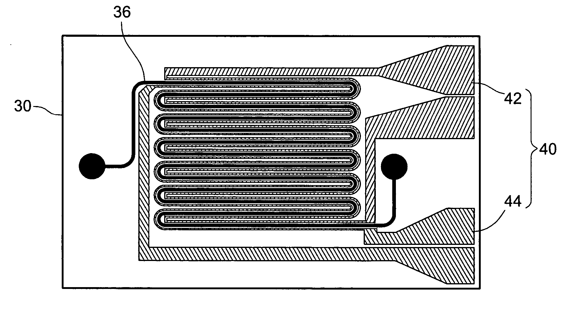
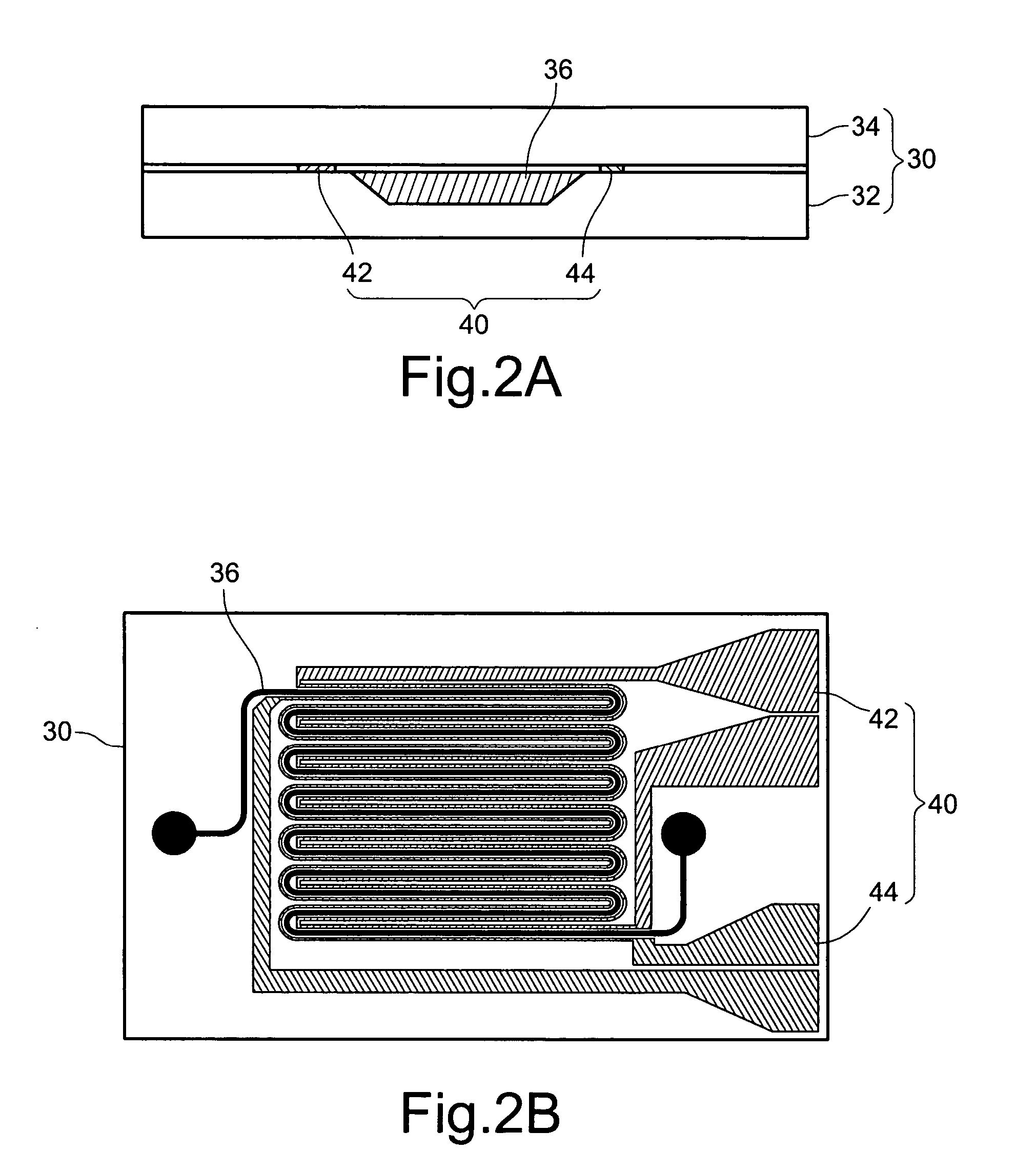
[0027] Firstly, refer to FIG. 2A and 2B for the schematic diagrams of the cross section view and plane view respectively of the microfluidic chip according to the invention. Said microfluidic chip can be utilized in the chain reactions of the growth of the poly-enzyme mainly including: a main body 30 and an electrode layer 40. The main body 30 includes a first substrate 32 and a second substrate 34. A serpentine-winding shape microchannel 36 is provided on the first substrate 32, which can be used to contain the test fluid flowing therein for the experimental analysis of the cell or the sample body, by taking advantage of its feature of miniature size and fast reaction speed. For the requirement of optical observation, the main body 30 is made of glass material, having a good light transmission capability, as such facilitating the optical observation of the processing and the operation of the test fluid.

[0028] In practice, the electrode layer 40 is made of metal having a melting poi...

second embodiment

[0035] In addition, in order to increase the product utilization rate of a single wafer to reduce the production cost, the 6 mircochannel-electrode-on-chip structures, originally designed to be placed on a 4-inch wafer, are increased to 12 the mircochannel-electrode-on-chip structures. As shown in FIG. 4, it illustrates the schematic diagram of the plane view of the mircochannel-electrode-on-chip structure according to the invention. In order to obtain the optimal design, the width and the spacing of the electrode layer 50 (including the heater wire 52 and the sensor wire 54) are changed respectively, to realize the optimized temperature variations.

[0036] Moreover, in order to fully understand the effect of utilizing the various metals as the material of the electrode layer, experiments are conducted for varying the metal utilized for the electrode layer of the microfluidic chip. So chromium (Cr), gold (Au), titanium (Ti), and platinum (Pt) are sputtered respectively on the glass su...

third embodiment

[0038] In the invention, the heater wire and the sensor wire are disposed respectively along the main body on either side of the microchannel.

[0039] However, in practical applications, other designs are possible, as long as the heater wire is disposed in the vicinity of the microchannel. For example, as shown in FIG. 6A, the heater wire 70 is provided at the backside of the microchannel 72, thus constituting the fourth embodiment of the invention. In addition, as shown in FIG. 6B, the heater wire 80 is provided at the opposite side of the microchannel 82, thus constituting the fifth embodiment of the invention.

[0040] Besides, one-sided or two-sided of the main body may be made of the transparent material selected from the group including of glass, rock crystals, plastics, resins, photo resists, transparent ceramics and synthetic materials thereof. The one-sided transparent main body limits the observation scope, and the two-sided transparent main body is provided for the front and ...


PUM

PropertyMeasurementUnit
melting pointaaaaaaaaaa
transparentaaaaaaaaaa
temperatureaaaaaaaaaa

Abstract

A microfluidic chip on a transparent substrate includes microchannels, and an electric layer having a heater and a sensor layout on the microchannel nearby and aside for supplying heat source and sensing the temperature individually. The sensor is close to the microchannel for controlling the temperature accurately. Hence, the microfluidic chip can measure the temperature precisely without using an isolation layer and lower energy consumptions and reduce production costs.

Description

BACKGROUND [0001] 1. Field of the Invention [0002] The invention relates to a microfluidic chip, which is utilized in a poly-enzyme chain reaction and hybrid array of biochemical experiments, and in particular to a microfluidic chip, which can be utilized to raise the efficiency of biochemical reactions. [0003] 2. Related Art [0004] The poly-enzyme chain reaction is presently the most frequently used method for nucleotide multiplication and augmentation. The quantity of DNA(deoxyribonucleic acid) can be multiplied exponentially several million times through the repeated denatured, annealing and extension processes of the segments of DNA, by thermal circulation, so that the traditional time consuming process of bio-medical sample body treatment and its reaction schedule can be shortened significantly. [0005] In the poly-enzyme chain reaction, the sample body must be augmented through a micro channel-electrode-on-chip device having electrodes and micro-channel disposed thereon, to spe...

Claims


Application Information

Patent Timeline
Patent Type & Authority Applications(United States)
IPC IPC(8): G01N33/00
CPCB01L3/502707B01L7/52B01L2200/147B01L2300/0816B01L2300/1827G01N27/44704
Inventor PARNG, SHAW-HWAYU, TUNG-MING
Owner IND TECH RES INST
Why Eureka
Try Eureka