Multi-band highly reflective flexible wave plate and preparation method thereof

A high-reflection, multi-band technology, applied in the direction of instruments, polarizing elements, optics, etc., can solve the problems of complex process, low reflectivity, non-bendable nature, etc., and achieve good application prospects and simple production effects

Active Publication Date: 2020-10-16
SHANGHAI INST OF OPTICS & FINE MECHANICS CHINESE ACAD OF SCI
View PDF10 Cites 0 Cited by
  • Summary
  • Abstract
  • Description
  • Claims
  • Application Information

AI Technical Summary

Problems solved by technology

[0004] Based on the above structures, there are generally disadvantages such as single-band limitation and low reflectivity; most of the designs are two-dimensional structures, which need to be fabricated by etching metal
Due to the difficulty of metal etching, the above-mentioned structures have the problems of complicated process and difficult fabrication.
In addition, this type of wave plate uses hard substrates such as silica, alumina, and silicon materials, which are not bendable, so they cannot meet the applications of wearable and flexible devices.

Method used


Image

  • Multi-band highly reflective flexible wave plate and preparation method thereof
  • Multi-band highly reflective flexible wave plate and preparation method thereof
  • Multi-band highly reflective flexible wave plate and preparation method thereof

Examples


Embodiment

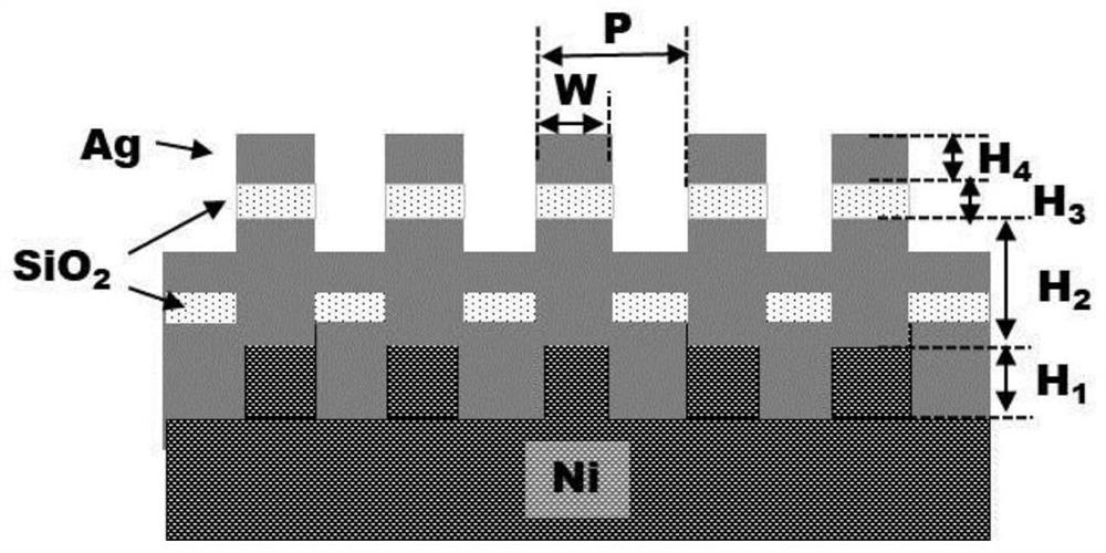
[0029] see figure 1 , the embodiment of the multi-band highly reflective flexible wave plate of the present invention includes a substrate with a nano-metal nickel grating, and a first silver metal layer, a silicon dioxide resonant cavity layer and a second silver metal layer are sequentially arranged on the upper layer of the substrate. The resonant cavity medium layer and the second metal layer are discontinuously distributed in the grating groove and grid ridge position of the base nickel grating, the period P of the nano-metal nickel grating is 250nm, and the duty ratio W / P is 0.5, the thickness H1 is 140nm; the thickness H2 of the first metal layer is 160nm, the thickness H3 of the resonant cavity medium layer is 50nm, and the thickness H4 of the second metal layer is 50nm.

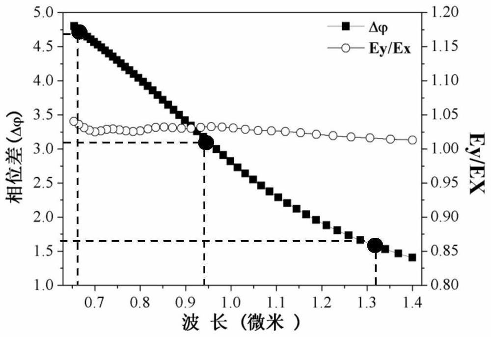
[0030] see figure 2 , the material of the dielectric grating in this embodiment is SiO 2 , the material of the metal layer is Ag. is the phase difference of the polarization components in Ex and...


PUM

PropertyMeasurementUnit
thicknessaaaaaaaaaa
thicknessaaaaaaaaaa
thicknessaaaaaaaaaa

Abstract

The present invention provides a multi-waveband high-reflection flexible wave plate and a preparation method thereof. The structure of the multi-waveband high-reflection flexible wave plate comprisesa nano metallic nickel optical grating substrate, the nano metallic nickel optical grating substrate is provided with a first metal layer, a medium resonant cavity layer and a second metal layer in order, the first metal layer is continuous, namely, and the substrate optical grating groove is completely filled; and the resonant cavity layer and the second metal layer are discontinuously distributed at the substrate nickel optical grating optical grating groove and the grating ridge. The multi-waveband high-reflection flexible wave plate is prepared by combination of a traditional dual-beam exposure technology and an electroforming process and is subjected to large-area preparation by employing a traditional process to achieve functions of 1 / 2 and 1 / 4 wave plates at different wave bands. The multi-waveband high-reflection flexible wave plate has multi-waveband, high-reflection and flexible performances, does not etching of metal, is simple to manufacture, and can be used at the aspectsof flexible display and wearable flexible products.

Description

technical field [0001] The invention relates to a polarization optical element, in particular to a surface plasmon resonance-based multi-band high-reflection flexible wave plate and a preparation method thereof. Background technique [0002] In the field of research and application of light, the generation and conversion control of the polarization state of light is very important. Polarization is the property of the wave plate. Most of the traditional devices for generating and controlling the polarization state of light use birefringent crystal materials. When the light is incident on the birefringent crystal, due to the different The optical refractive index, so when light passes through a birefringent crystal, the transmitted light will have a phase difference in these two orthogonal directions, thereby changing the polarization state of the light. As an important optical device, the traditional crystal wave plate is limited by its physical size, which makes it difficul...

Claims


Application Information

Patent Timeline
Patent Type & Authority Patents(China)
IPC IPC(8): G02B5/30
CPCG02B5/3083
Inventor 胡敬佩朱玲琳张方曾爱军黄惠杰
Owner SHANGHAI INST OF OPTICS & FINE MECHANICS CHINESE ACAD OF SCI
Why Eureka
Try Eureka