Liquid crystal display device with touch panel and manufacturing method thereof

A liquid crystal display device, touch panel technology, applied in the input/output process of data processing, instruments, polarizing elements, etc., can solve the problem of inability to obtain front contrast, and achieve the effect of excellent front contrast

Active Publication Date: 2021-02-02
KONICA MINOLTA INC
View PDF47 Cites 0 Cited by
  • Summary
  • Abstract
  • Description
  • Claims
  • Application Information

AI Technical Summary

Problems solved by technology

[0012] The inventors of the present invention combined the above-mentioned so-called mid-cell type or built-in polarizer-integrated touch panel module with a VA mode liquid crystal display unit. The improvement effect of frontal contrast

Method used


Image

  • Liquid crystal display device with touch panel and manufacturing method thereof
  • Liquid crystal display device with touch panel and manufacturing method thereof
  • Liquid crystal display device with touch panel and manufacturing method thereof

Examples


preparation example Construction

[0324] The thickness of the film can be prepared by adjusting the solid concentration contained in the dope, the slit gap of the nozzle of the die, the extrusion pressure from the die, the speed of the metal support, etc. so as to obtain a desired thickness. The width of the transparent resin film obtained as described above is preferably in the range of 0.5 to 4 m, more preferably in the range of 0.6 to 3 m, and even more preferably in the range of 0.8 to 2.5 m. The length is preferably wound in the range of 100 to 10,000 m per roll, more preferably in the range of 500 to 9,000 m, and still more preferably in the range of 1,000 to 8,000 m.

[0325] The optical compensation film involved in the present invention can achieve desired optical properties by properly adjusting the process conditions such as the polymer structure used, the type and amount of additives, stretching ratio, and residual volatile components during peeling.

[0326] The optical compensation film according...

Embodiment 1

[0433] As the cellulose ester-based resin, cycloolefin-based resin, polyimide-based resin, polyarylate-based resin, and acrylic resin used in Examples, resins listed below were used.

[0434] [resin]

[0435] Cycloolefin-based resin (COP): ARTON G7810, manufactured by JSR Corporation

[0436] Cellulose acetate propionate (CAP): acetyl substitution degree 1.5, propionyl substitution degree 1.0, total acyl substitution degree 2.5, weight average molecular weight 250,000)

[0437] Polyimide-based resin (PI): A polyimide-based resin was synthesized by the following method.

[0438]

[0439] (polymerization of polyimide precursor)

[0440] Production of polyamic acid using a reactor equipped with a stainless steel separable flask as a reaction vessel, 2 paddle fins as a stirring device in the separable flask, and a device with a cooling capacity of 20.9 kJ / min as a cooling device . During the polymerization reaction, in order to prevent the incorporation of moisture, nitrogen...

Embodiment 2

[0560]

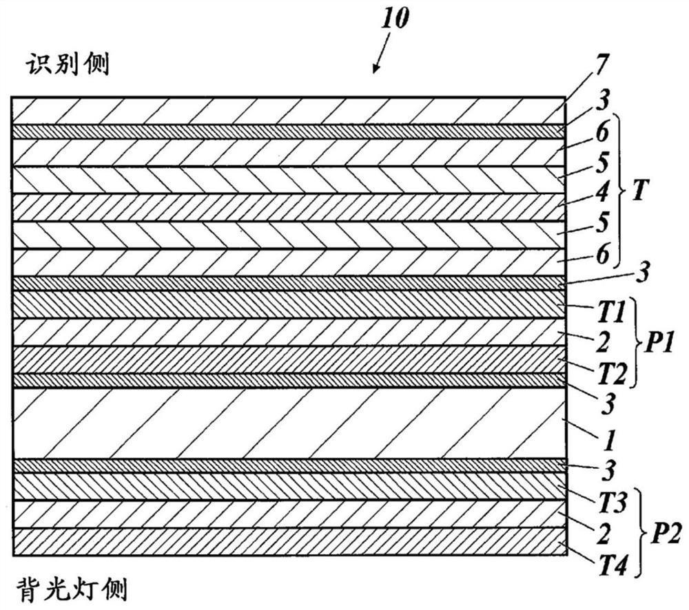
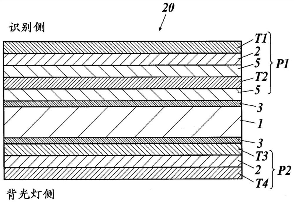
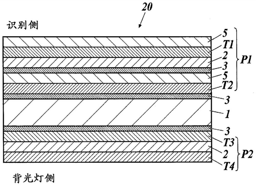
[0561] One side of the optical compensation films 104, 110, 112 and 114 related to the present invention made in Example 1 is formed with an ITO film as a transparent conductive layer with a thickness of 20 nm by the sputtering method, and forms the first layer in the X direction by etching. 1 electrode pattern.

[0562] Next, as an insulating layer arranged between the electrode patterns, SiO 2 A film was formed, an ITO film was formed thereon by sputtering so as to have a thickness of 20 nm, and a second electrode pattern was formed in the Y direction by etching. Furthermore, SiO was sputtered to a thickness of 200nm 2 Formed into a film as an insulating layer. Next, heat treatment (annealing) was performed at 150° C. for 30 minutes to lower the resistance value, and optical compensation films 201 to 204 having transparent conductive layers corresponding to optical compensation films 104 , 110 , 112 , and 114 were produced.

[0563] Image 6 >

[0564] The pol...


PUM

PropertyMeasurementUnit
glass transition temperatureaaaaaaaaaa
thicknessaaaaaaaaaa
glass transition temperatureaaaaaaaaaa

Abstract

An object of the present invention is to provide a liquid crystal display device with a touch panel having a VA-mode liquid crystal cell excellent in front contrast, and a method for manufacturing the same. The liquid crystal display device with a touch panel of the present invention is a liquid crystal display device with a touch panel provided with a polarizer-integrated touch panel module having a transparent conductive layer on the identification side of a VA mode liquid crystal cell, and is characterized in that The polarizer-integrated touch panel module having the above-mentioned transparent conductive layer has an optical compensation film having a transparent conductive layer on at least one side, a polarizer, and a protective film in order from the above-mentioned VA-mode liquid crystal cell to the identification side, and the above-mentioned optical compensation film The glass transition temperature Tg is in the range of 155-250°C.

Description

technical field [0001] The invention relates to a liquid crystal display device with a touch panel and a manufacturing method thereof. In more detail, it is related with the liquid crystal display device with a touch panel excellent in front contrast, and its manufacturing method. Background technique [0002] In recent years, the popularity of liquid crystal display devices equipped with touch panels has been increasing, and it is expected to continue to increase in the future. [0003] For example, in a capacitive touch panel module used in a touch panel, an X electrode pattern extending in the X direction using a transparent conductive layer (also referred to as a transparent electrode) is formed on a transparent substrate, and an X electrode pattern using another transparent conductive layer is formed. A Y electrode pattern extending in the Y direction. When the surface of the touch panel is touched with a finger, the X electrode pattern comes into contact with the Y e...

Claims


Application Information

Patent Timeline
Patent Type & Authority Patents(China)
IPC IPC(8): G02F1/1333G02B5/30G02F1/1335G02F1/13363G06F3/041G06F3/044
CPCG02F1/1333G02F1/1335G02F1/13363G02B5/30G06F3/041G06F3/0445G06F2203/04103
Inventor 森井里志
Owner KONICA MINOLTA INC
Why Eureka
Try Eureka