Fault injection design and verification method of memory with EDAC error tolerance

A technology of fault injection and verification method, which is applied in the direction of static memory, general-purpose stored program computer, and architecture with a single central processing unit, etc. It can solve undiscovered problems, ensure consistency, improve reliability, and simple fault injection method clear effect

Active Publication Date: 2018-11-06
XIAN MICROELECTRONICS TECH INST
View PDF3 Cites 7 Cited by
  • Summary
  • Abstract
  • Description
  • Claims
  • Application Information

AI Technical Summary

Problems solved by technology

In particular, how to realize the fault-injection design and verification of fault-tolerant memor

Method used


Image

  • Fault injection design and verification method of memory with EDAC error tolerance

Examples


Embodiment Construction

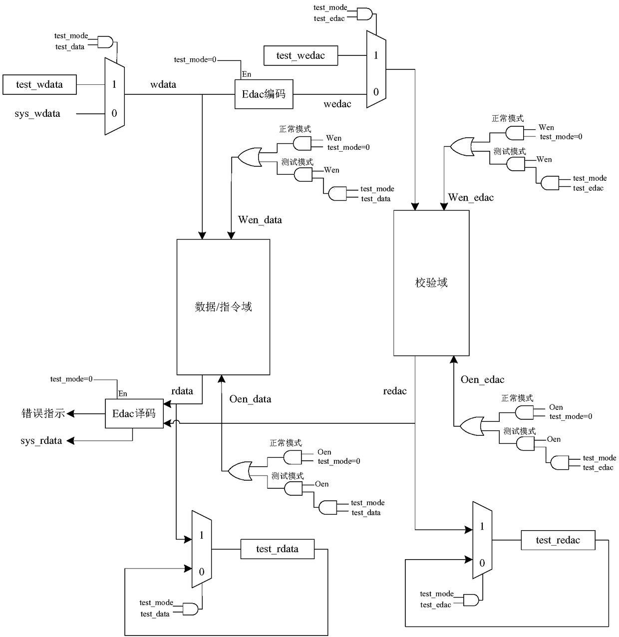
[0032] The invention provides an EDAC fault-tolerant memory fault injection design and verification method, which is used for independently realizing fault injection and verification of the data / instruction domain and the check domain of the fault-tolerant memory.

[0033] A kind of memory fault injection design and verification method with EDAC fault tolerance of the present invention, comprises the following steps:

[0034] S1. For the read and write access of the data / command field and the check field, the working mode is divided into different controls;

[0035] In normal working mode, the data / command field and the check field read and write access control signals and control timing are consistent, and there is no need to set an independent access control signal for the check field, and it is not necessary to allocate additional The access address, the data / instruction field and the verification field are in one-to-one correspondence, just use the same address as the data...


PUM


Abstract

The invention discloses a fault injection design and verification method of a memory with EDAC error tolerance. Reading and writing access of a data/instruction domain and a check domain is controlleddifferently according to working modes, in the test mode, during reading operation of the data/instruction domain, a control signal of the reading operation of the data/instruction domain is only effective, and test reading access of the data/instruction domain is realized; during reading operation of the check domain, a control signal of the reading operation of the check domain is only effective, and test reading access of the check domain is realized; during fault injection of the data/instruction domain, a control signal of the writing operation of the data/instruction domain is only effective; during fault injection of the check domain, a control signal of writing operation of the check domain is only effective, and any fault injection of the data/instruction domain and the check domain is realized. Independent reading and writing access of the data/instruction domain and the check domain is realzied, and testability of the memory after error tolerance design is guaranteed.

Description

technical field [0001] The invention belongs to the technical field of integrated circuit design, and in particular relates to a memory fault injection design and verification method with EDAC fault tolerance. Background technique [0002] The SEU (Single-Event-Upset) effect in the space environment can easily affect digital integrated circuit components, especially memory devices, resulting in program execution errors and system failure. The memory can be located on the SoC (System onChip) chip, or it can be located outside the SoC as its external storage space, but the memory controller is generally located in the SoC. For the practical application of the space environment, in order to improve the radiation resistance of the SoC main memory system, the on-chip memory and the off-chip memory need to adopt a fault-tolerant reinforcement design. Since the main memory system is not reproducible, EDAC coding is usually used, making most of the errors The purpose of correct rep...

Claims


Application Information

Patent Timeline
IPC IPC(8): G11C29/10G06F15/78
CPCG06F15/7807G11C29/10
Inventor 崔媛媛张海金娄冕王会敏马子轩刘虎兵
Owner XIAN MICROELECTRONICS TECH INST
Why Eureka
Try Eureka