SONOS memory and preparation method thereof

A technology of memory and charge storage layer, which is applied in the direction of electric solid-state devices, semiconductor devices, electrical components, etc., can solve the problem that the data retention ability needs to be improved, and achieve the effect of improving the data retention ability

Inactive Publication Date: 2018-11-06
SHANGHAI HUALI MICROELECTRONICS CORP
View PDF8 Cites 0 Cited by
  • Summary
  • Abstract
  • Description
  • Claims
  • Application Information

AI Technical Summary

Problems solved by technology

[0004] However, the data retention capability of th

Method used


Image

  • SONOS memory and preparation method thereof
  • SONOS memory and preparation method thereof
  • SONOS memory and preparation method thereof

Examples


Example Embodiment

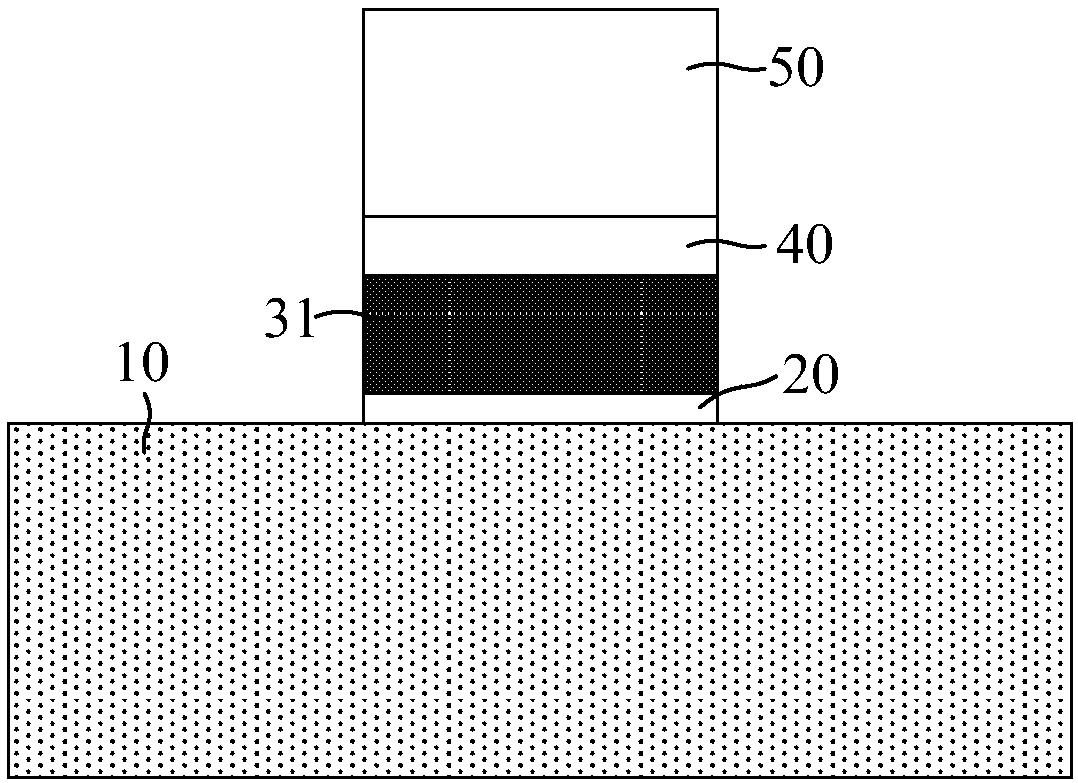
[0033] figure 1 It is a cross-sectional view of a typical SONOS memory structure. like figure 1 As shown, a typical SONOS memory structure is composed of silicon substrate 10(S)-tunneling oxide layer 20(O)-charge storage layer silicon nitride 30(N)-blocking oxide layer 40(O)-polysilicon gate 50( S) composition. The storage principle of the SONOS memory structure is that electrons and holes in the substrate tunnel through the oxide layer under the action of gate bias to realize data writing and erasing.

[0034] However, the inventor found that the data retention of the SONOS memory is carried out without power supply, and with the growth of time, the electrons or holes stored in the silicon nitride layer film continue to overflow, resulting in data loss. Therefore, a charge storage layer with stronger charge storage capacity is required to improve the charge storage capacity of the SONOS memory.
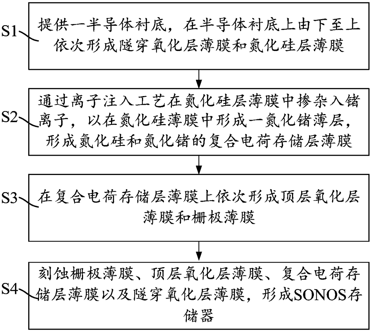
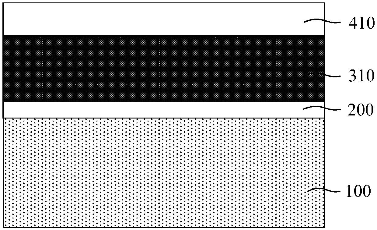
[0035] Based on the above findings, embodiments of the present invention pro...


PUM


Abstract

The invention provides a SONOS memory and a preparation method thereof. The method comprises the following steps: providing a semiconductor substrate, orderly forming tunneling oxide layer film and asilicon nitride layer film on the semiconductor substrate from bottom to top; doping germanium ion in the silicon nitride layer film through an ion injection process, thereby forming a germanium nitride thin layer in the silicon nitride film, and forming a composite charge storage layer film of the silicon nitride and the germanium nitride; orderly forming a top oxide layer film and a grid film onthe composite charge storage layer film; etching the grid film, the top oxide layer film, the composite charge storage layer film and the tunneling oxide layer film, and forming the SONOS memory. Thecharge storage layers of the germanium nitride and silicon nitride are used as the charge storage layer in the SONOS memory, the charge capturing and storing capacity are improved, and the data holding capacity of the SONOS memory is improved.

Description

technical field [0001] The invention relates to the field of semiconductor integrated circuit manufacturing, in particular to a SONOS memory and a preparation method thereof. Background technique [0002] Traditional polysilicon floating gate memories use floating gates (floating gate electrodes) to store data, and since doped polysilicon is a conductor, the charges stored in the floating gates are continuously distributed. When the size of the floating gate memory is scaled down, the size of the insulating layer around the floating gate is also reduced accordingly, and the reduction of the size of the insulating layer will cause the electrons in the polysilicon floating gate to be easily lost. When a certain part of the polysilicon floating gate leaks electricity, that is, there is a leakage channel, the charges stored in the entire polysilicon floating gate will be lost through the leakage channel. That is to say, the biggest obstacle restricting the scaling down of float...

Claims


Application Information

Patent Timeline
IPC IPC(8): H01L27/11568
CPCH10B43/30
Inventor 章晶唐小亮黄冠群
Owner SHANGHAI HUALI MICROELECTRONICS CORP
Why Eureka
Try Eureka