Intelligent selection method and device for two-dimensional MEMS OSW optical switch Hitless point

An intelligent selection and optical switch technology, applied in the field of optical communication, can solve the problems of screening efficiency and accuracy that cannot meet mass production, reduce the screening yield of optical switch modules, and optical signal interference, etc., to achieve mass production and improve Screening efficiency and accuracy, the effect of reducing labor intensity

Active Publication Date: 2018-11-06
GUANGXUN SCI & TECH WUHAN
View PDF6 Cites 7 Cited by
  • Summary
  • Abstract
  • Description
  • Claims
  • Application Information

AI Technical Summary

Problems solved by technology

However, the screening efficiency and accuracy of this manual screening method cannot meet the requirements of mass production; moreover, in the channel switching of the MEMS OSW optical switch, it is completed from the Hitless point to each channel in an approximately

Method used


Image

  • Intelligent selection method and device for two-dimensional MEMS OSW optical switch Hitless point
  • Intelligent selection method and device for two-dimensional MEMS OSW optical switch Hitless point
  • Intelligent selection method and device for two-dimensional MEMS OSW optical switch Hitless point

Examples


Embodiment 1

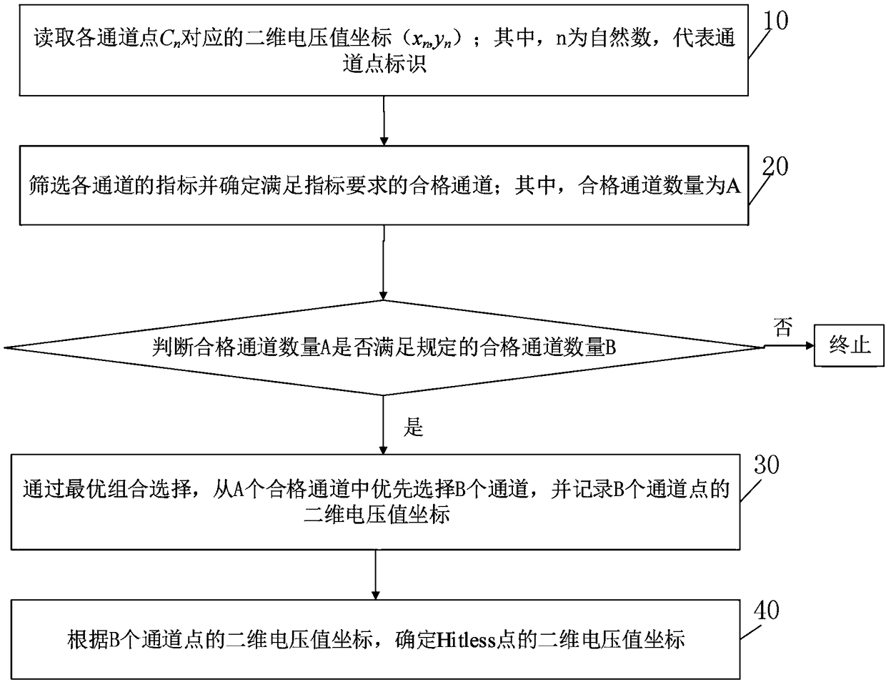
[0058] Embodiment 1 of the present invention provides an intelligent selection method for a two-dimensional MEMS OSW optical switch hitless point, such as figure 1 shown, including the following steps:

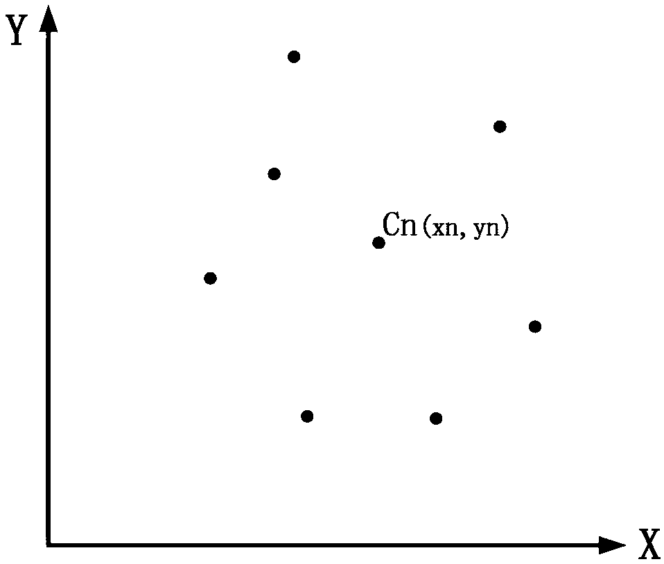
[0059] Step 10, read each channel point C n The corresponding two-dimensional voltage value coordinates (x n ,y n ); wherein, n is a natural number, representing the channel point identifier.

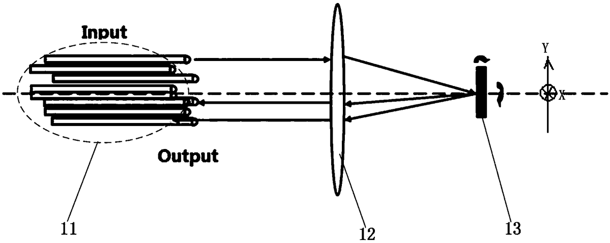
[0060] In the embodiment of the present invention, a two-dimensional 1×N MEMS OSW optical switch is used, which corresponds to 1 input port and N output ports, so there are N+1 optical channels in total, such as figure 2 As shown, the optical switch used in the embodiment of the present invention includes a single-mode optical fiber 11, a lens 12, and a two-dimensional MEMS rotating mirror 13, wherein, on the left side are N+1 single-mode optical fibers 11, and each single-mode optical fiber 11 corresponds to a light Channels, one of which is an input terminal, and the remaining N ...

Embodiment 2

[0078]On the basis of the above-mentioned embodiment 1, the embodiment of the present invention also provides another intelligent selection method for the hitless point of the two-dimensional MEMS OSW optical switch. The main difference from the embodiment 1 lies in the addition of identifying the interference channel point and setting the transit point The steps are applicable to the situation where there are interference channel points on the switching path from the Hitless point to one of the channel points. By setting the transit point, it is possible to bypass the interference channel point and switch to other channel points from the Hitless point in the form of a polyline path. , avoiding the occurrence of optical signal interference in the channel switching process, ensuring the switching response time and improving the screening yield of the optical switch module.

[0079] Such as Figure 9 As shown, the Hitless point intelligent selection method provided by the embodi...

Embodiment 3

[0099] On the basis of the method for intelligently selecting the hitless point of a two-dimensional MEMS OSW optical switch provided in embodiment 1 and embodiment 2, the present invention also provides a method for intelligently selecting the hitless point of the two-dimensional MEMS OSW optical switch using the above method devices such as Figure 12 Shown is a schematic diagram of the device architecture of the embodiment of the present invention. The two-dimensional MEMS OSW optical switch Hitless point intelligent selection device of this embodiment includes one or more processors 21 and memory 22 . in, Figure 12 A processor 21 is taken as an example.

[0100] The processor 21 and the memory 22 may be connected via a bus or in other ways, Figure 12 Take connection via bus as an example.

[0101] The memory 22 is a two-dimensional MEMS OSW optical switch Hitless point intelligent selection method and device non-volatile computer-readable storage medium, which can be...


PUM


Abstract

The invention relates to the technical field of optical communications, and in particular, to an intelligent selection method and an intelligent selection device for a two-dimensional MEMS OSW opticalswitch Hitless point, wherein the method comprises: reading a two-dimensional voltage value coordinate (xn, yn) corresponding to each channel point Cn; screening the indicators of each channel and determining the qualified channels satisfying the requirements of the indicators; preferentially selecting B channels from the A qualified channels; and determining the two-dimensional voltage value coordinate of the Hitless point according to the two-dimensional voltage value coordinates of the B channel points. In the intelligent selection method of the two-dimensional MEMS OSW optical switch Hitless point provided by the invention, the computer may quickly and intelligently select the optimal B channels and determine the Hitless point according to the optimal B channels and the selection ruleof the Hitless point, which replaces the traditional manual screening process, greatly improves the screening efficiency and accuracy, reduces the labor intensity of manual screening, and may realizemass production. When an interference channel point exists, a transit point is also set to avoid the emergence of the optical signal interference during channel switching.

Description

【Technical field】 [0001] The invention relates to the technical field of optical communication, in particular to an intelligent selection method and device for a hitless point of a two-dimensional MEMS OSW optical switch. 【Background technique】 [0002] Optical switches and optical switch arrays are key devices in Optical Add-Drop Multiplexer (OADM) equipment, Optical Cross-Connect (OXC) equipment and optical routing equipment, with control signals in The function of on-off and wavelength conversion between the same channel or different channels is of great significance to solve the wavelength contention in the current complex network, improve the wavelength reuse rate and flexibly configure the network. [0003] As a new type of optical switch in the optical switch series, the two-dimensional microelectromechanical system optical switch (MicroElectroMechanical System Optical SWitch, abbreviated as MEMS OSW) has the characteristics of small size, low cost, low power consumpt...

Claims


Application Information

Patent Timeline
IPC IPC(8): H04B10/073H04Q11/00
CPCH04B10/0731H04Q11/0005H04Q2011/003
Inventor 杨波郑洁何俊罗勇尹轶群
Owner GUANGXUN SCI & TECH WUHAN
Why Eureka
Try Eureka