High density photon integrated waveguide grating array

A waveguide grating and waveguide technology, applied in the field of optoelectronic integrated devices and preparation, can solve the problems of low crosstalk between waveguides, and achieve the effect of high scanning range and precision

Active Publication Date: 2018-11-09
江伟
View PDF24 Cites 5 Cited by
  • Summary
  • Abstract
  • Description
  • Claims
  • Application Information

AI Technical Summary

Problems solved by technology

For high-density waveguide arrays with waveguide spacing close to or smaller than the wavelength, it is difficul

Method used


Image

  • High density photon integrated waveguide grating array
  • High density photon integrated waveguide grating array
  • High density photon integrated waveguide grating array

Examples


Example Embodiment

[0035] 【Example 1】

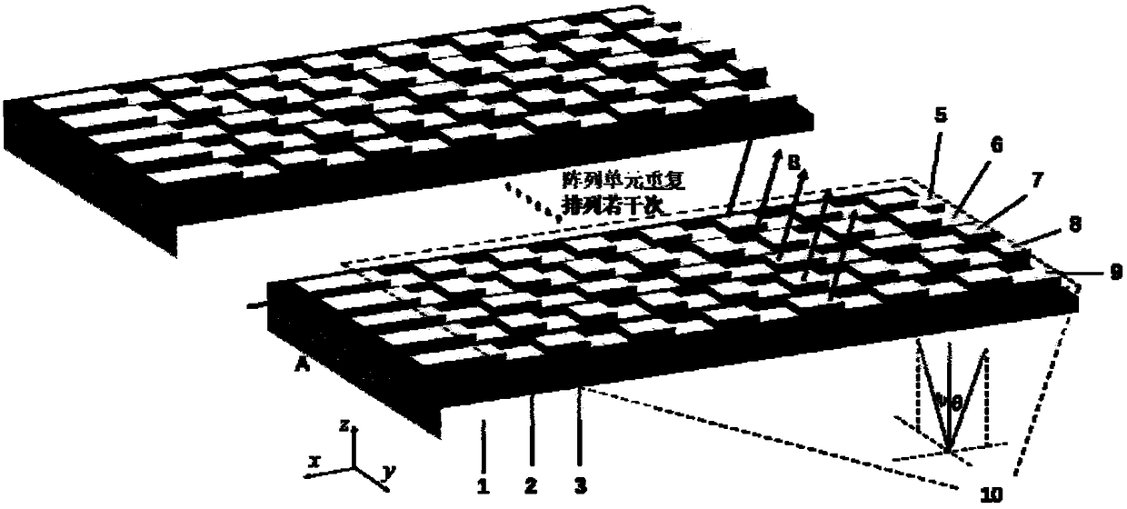
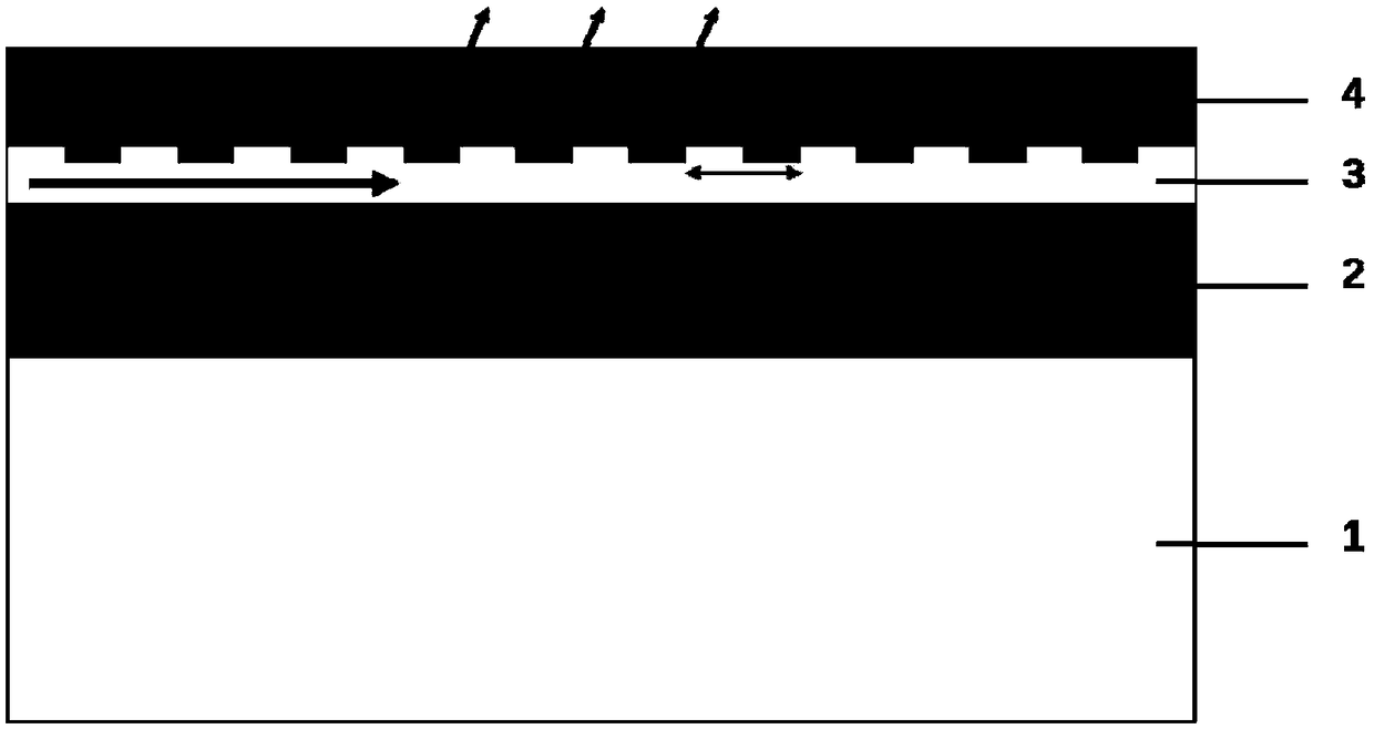
[0036] High-density optical phased array antenna arrays are implemented on silicon-on-insulator (SOI), such as figure 1 shown. The structure can be divided into four layers: a silicon substrate 1 , a silicon oxide layer 2 , a silicon layer 3 defining the device, and a top-covering silicon dioxide layer 4 , on which the bulk of the device rests. The phased array antenna array is composed of four repeated array units 10, and each array unit includes five different waveguide gratings 5-9. These five different waveguide gratings have different waveguide widths, so that the waveguide modes have different Spread constant. In this example light propagates in the waveguide along the x-axis direction (-x direction to be exact). where the grating structure is obtained by etching13,14. Each grating has a different period to ensure that the optical signal exits at the same angle. The specific relationship can be obtained by the following formula:

[0037]

[...

Example Embodiment

[0039] [Example 2]

[0040] The number of array units is not limited to four, and can be increased or decreased according to requirements, for example, 3-1000. The number of waveguide gratings in each array unit is not limited to five, for example, 2-20.

Example Embodiment

[0041] [Example 3]

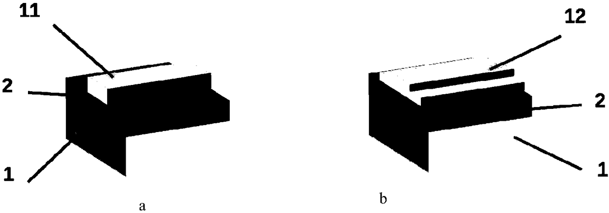
[0042] The waveguide structure can use not only the strip waveguide 11, but also the ridge waveguide 12, or other waveguide forms.


PUM


Abstract

The invention provides a high density photon integrated waveguide grating array which is used for the device transmitting multipath optical signals. The high density photon integrated waveguide grating array comprises three or more parallel arranged waveguide gratings. The propagation constant of each waveguide grating is different from that of other adjacent waveguide gratings. The period of eachgrating is related to the propagation constant of the waveguide. The optical signals pass through different waveguide gratings and can be emergent at the same angle. The interval between the waveguide gratings is small so that the array is suitable for the optical phased array antenna. Large-angle transverse scanning is realized by changing the relative phase difference among all the waveguide gratings so as to have quite wide application prospect in the field of laser radar, medical imaging and wireless communication.

Description

technical field [0001] The invention relates to an optoelectronic integrated device and its preparation, especially a high-density photon integrated waveguide grating array. Background technique [0002] Silicon-based photonic devices have great application prospects in large-scale optoelectronic integration due to the advantage of low cost, and it is also an important means to realize optical phased arrays. Optical phased array has the characteristics of low cost, high speed, and high precision. It has important applications in lidar, medical imaging, wireless communication, etc. In order to further improve the scanning accuracy and scanning angle of the optical phased array, how to increase the density of the phased array antenna is an important problem to be solved. [0003] In the era of big data and artificial intelligence, autonomous driving technology has received extensive attention to solve the problem of traffic accidents caused by insufficient driving skills and ...

Claims


Application Information

Patent Timeline
IPC IPC(8): G02B6/12G02B6/124G02B6/125
CPCG02B6/12009G02B6/124G02B6/125
Inventor 江伟邵越冷乐蒙
Owner 江伟
Why Eureka
Try Eureka