Circuit board, semiconductor device, image capturing device, solid-state image capturing element, method of manufacturing solid-state image capturing element, and electronic instrument

一种固态图像、状态的技术,应用在半导体/固态器件制造、半导体器件、电气元件等方向,能够解决滤色器涂层不均匀等问题,达到减少涂布不均匀、抑制产量的降低、抑制特性的降低的效果

Active Publication Date: 2018-11-09
SONY CORP
View PDF12 Cites 0 Cited by
  • Summary
  • Abstract
  • Description
  • Claims
  • Application Information

AI Technical Summary

Problems solved by technology

Therefore, in the case of coating the color filter after forming the wiring portion, the coating of the color filter is uneven due to steps
[0005] In addition, for solid-state imaging devices such as front-illuminated CMOS image sensors and charge-coupled device (CCD) image sensors, a region where pixels are formed on a semiconductor substrate is formed in the wiring portion In the surrounding case, it is formed in such a way that the thickness of the wiring part is larger than the thickness of the area, and the coating of the color filter is uneven due to the step of the wiring part

Method used


Image

  • Circuit board, semiconductor device, image capturing device, solid-state image capturing element, method of manufacturing solid-state image capturing element, and electronic instrument
  • Circuit board, semiconductor device, image capturing device, solid-state image capturing element, method of manufacturing solid-state image capturing element, and electronic instrument
  • Circuit board, semiconductor device, image capturing device, solid-state image capturing element, method of manufacturing solid-state image capturing element, and electronic instrument

Examples


Embodiment Construction

[0054] Hereinafter, preferred embodiments of the present disclosure will be described in detail with reference to the accompanying drawings. It should be noted that, in this specification and the drawings, constituent elements that have substantially the same functional configuration will be denoted by the same reference numerals, and repeated description thereof will be omitted.

[0055]

[0056] In describing the configuration of the solid-state image sensor to which the technology of the present disclosure is applied, first, the mechanism by which the above-mentioned coating unevenness of the photoresist occurs will be described.

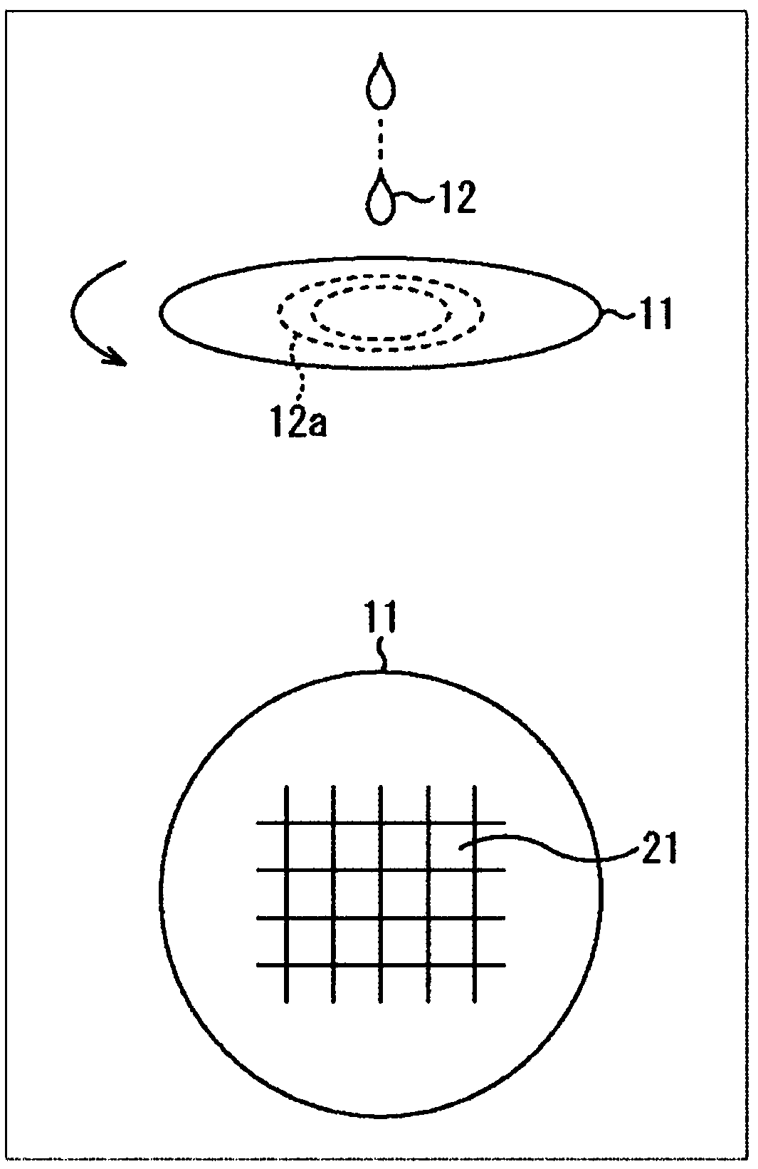
[0057] Coating unevenness of photoresist occurs in the photolithography process.

[0058] The photolithography process is a process for forming a pattern in which a photoresist layer is formed on a wafer containing a large number of solid-state image sensors before dicing, and the photoresist layer corresponding to the pattern is exposed by expos...


PUM


Abstract

The present disclosure relates to a circuit board, a semiconductor device, an image capturing device, a solid-state image capturing element, a method of manufacturing a solid-state image capturing element, and an electronic instrument which make it possible to suppress deterioration in characteristics and suppress a reduction in yield. A stepped part that forms on a substrate surface is configuredin a divided state. By this means, a photoresist liquid which is caused to drip during a lithography process flows through voids between the divided stepped parts, and thus flows uniformly with respect to an imaging surface, and it is thus possible to suppress a deterioration in characteristics due to sweep irregularities and a reduction in yield. The present disclosure can be applied to solid-state image capturing elements.

Description

technical field [0001] The present disclosure relates to a circuit board, a semiconductor device, an imaging device, a solid-state image sensor, a method of manufacturing a solid-state image sensor, and electronic equipment. Specifically, the present disclosure relates to a circuit board, a semiconductor device, an imaging device, a solid-state image sensor, a method of manufacturing a solid-state image sensor, and an electronic device that suppress a reduction in characteristics and suppress a reduction in yield. Background technique [0002] In recent years, there has been known a back-illuminated complementary metal oxide semiconductor (CMOS) image sensor having a layered structure in which a circuit board on which a driving circuit is formed is prepared in addition to a sensor board on which a photoelectric converter is formed, And the circuit board is bonded to the surface opposite to the light receiving surface of the sensor board. [0003] In this CMOS image sensor, ...

Claims


Application Information

Patent Timeline
Patent Type & Authority Applications(China)
IPC IPC(8): H01L27/146
CPCH01L21/0271G03F7/162H01L27/146H01L31/02366H01L21/0273H01L27/14632H01L27/14687
Inventor 竹尾建治
Owner SONY CORP
Why Eureka
Try Eureka