Semiconductor chip production technology
A production process and semiconductor technology, applied in the fields of semiconductor/solid-state device manufacturing, electrical components, circuits, etc., can solve problems such as affecting the grinding accuracy of silicon wafers, affecting the processing accuracy of silicon wafers, and inconvenient cleaning of silicon wafer powders, etc. Achieve the effect of improving grinding quality and improving safety
- Summary
- Abstract
- Description
- Claims
- Application Information
AI Technical Summary
Problems solved by technology
Method used
Image

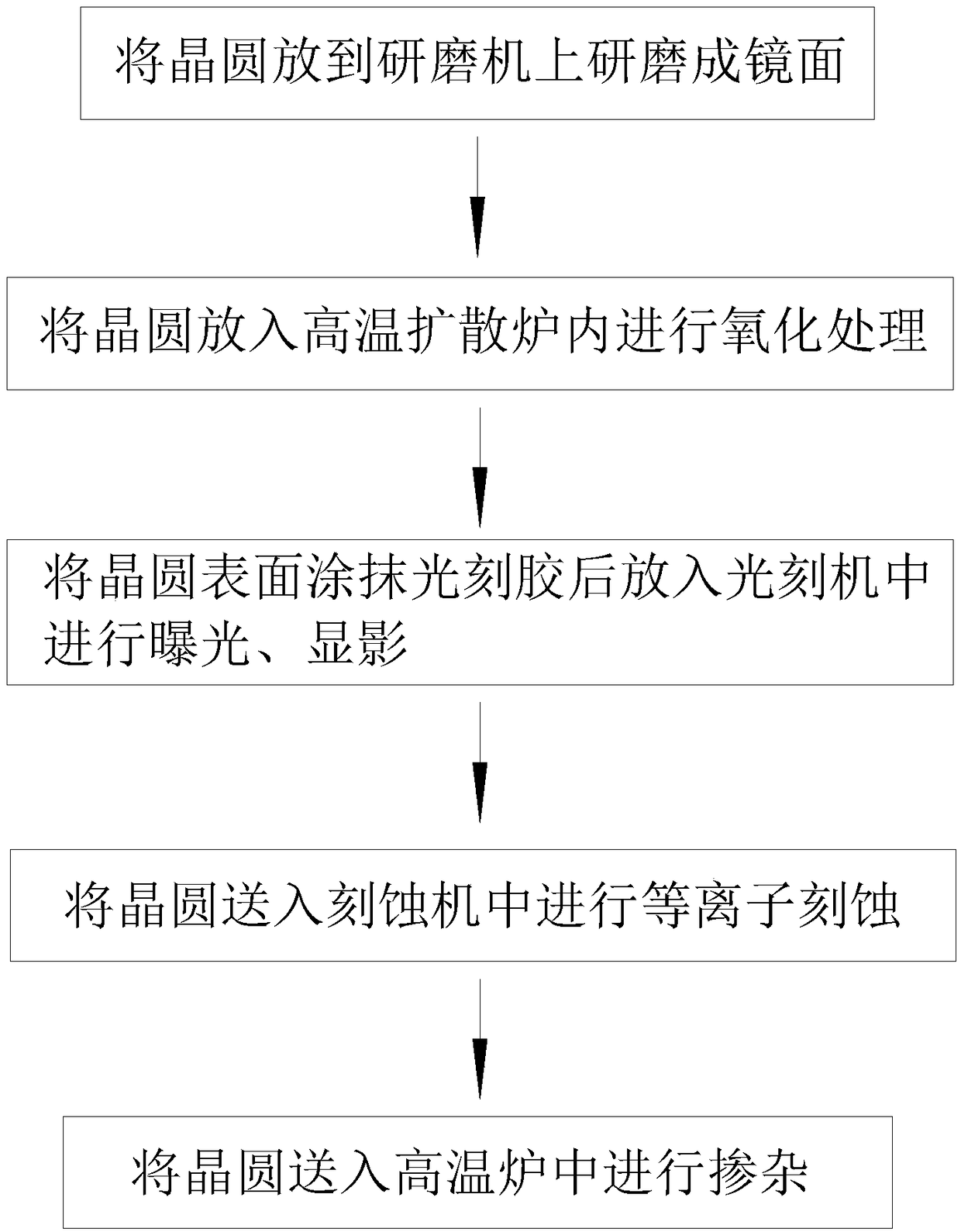
Examples
Embodiment approach
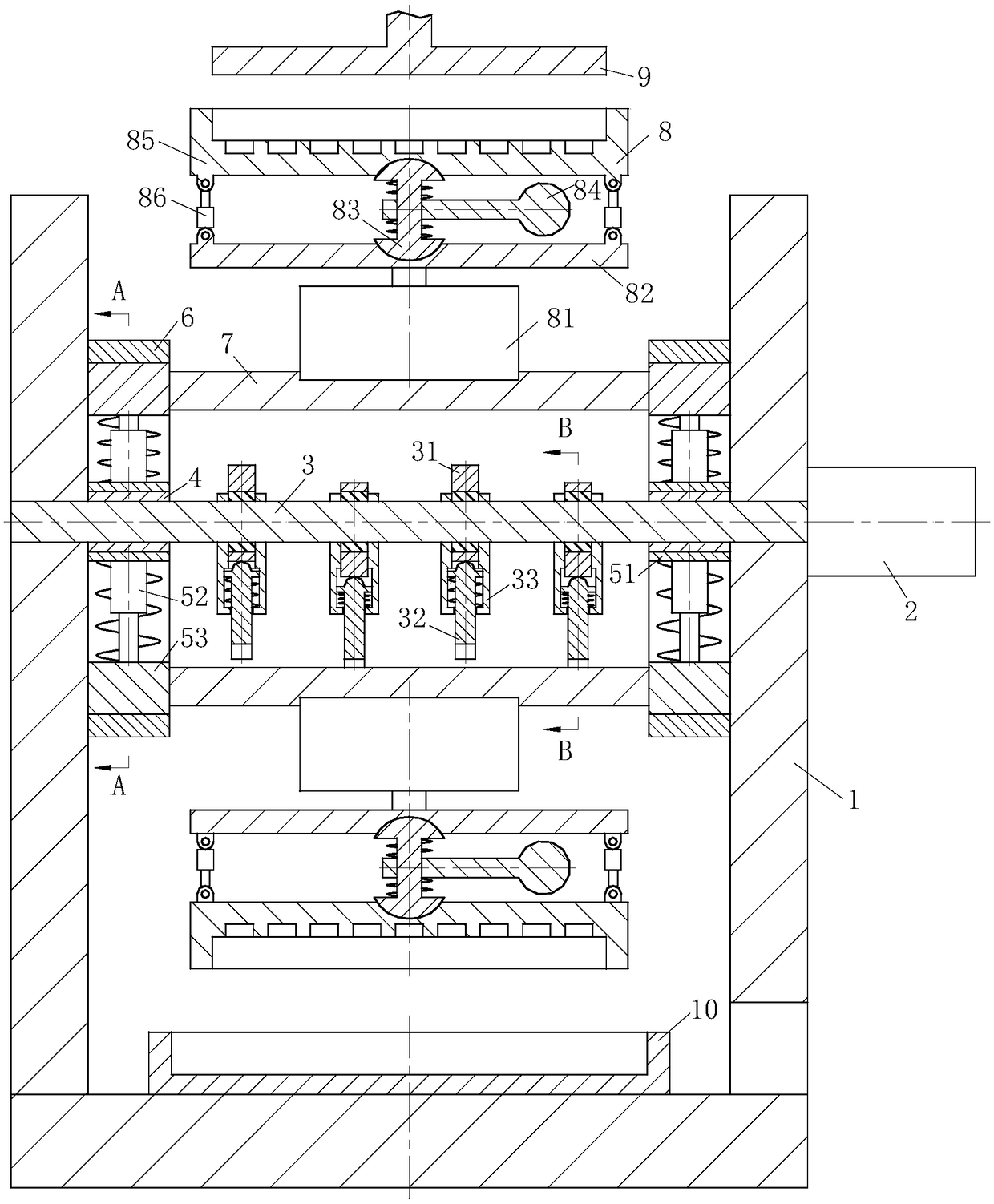
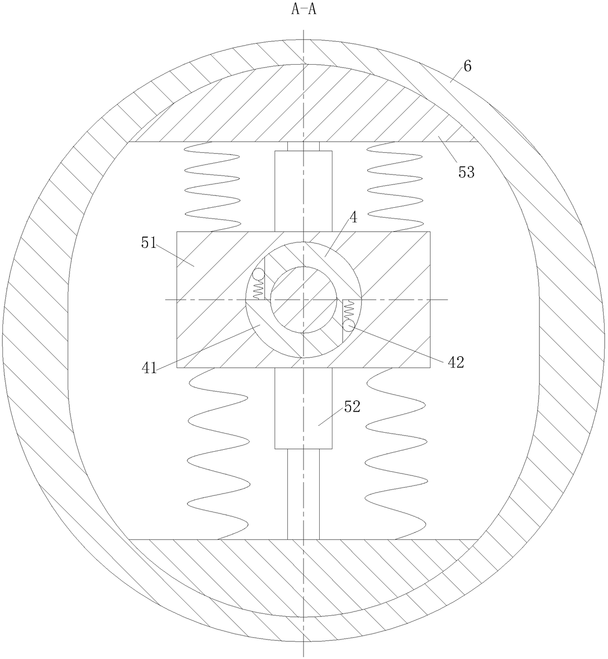
[0038] As an embodiment of the present invention, the grinding device 8 includes a grinding motor 81, a support disc 82, a transmission link 83, a counterweight rod 84, a spring, a grinding disc 85, and a No. 1 telescopic rod 86. The grinding motor 81 Fixedly connected to the middle part of the connecting rod 7, the shaft end of the grinding motor 81 is fixedly connected to the middle part of the support disc 82; the support disc 82 and the grinding disc 85 are hinged through a group of No. 1 telescopic rods 86, and a transmission is arranged above the middle part of the support disc 82. Connecting rod 83; the two ends of the transmission connecting rod 83 are arranged in an arc shape, and the middle part of the transmission connecting rod 83 is rotated to connect one end of the counterweight bar 84, and the transmission link 83 is provided with two springs; the counterweight bar 84 One end of it is kept suspended by two upper and lower springs, and the other end of the counter...
PUM
 Abstract
Description
Claims
Application Information