Semiconductor structures and methods of forming them

A technology of semiconductor and gate structure, which is applied in the field of semiconductor structure and its formation, can solve the problems such as the decline of electrical performance of semiconductor devices, and achieve the effects of avoiding adverse effects, increasing device speed, and improving electrical performance

Active Publication Date: 2020-10-09
SEMICON MFG INT (SHANGHAI) CORP +1
View PDF5 Cites 0 Cited by
  • Summary
  • Abstract
  • Description
  • Claims
  • Application Information

AI Technical Summary

Problems solved by technology

[0004] However, the introduction of the polysilicon interconnection layer will easily lead to a decrease in the electrical performance of the formed semiconductor device

Method used


Image

  • Semiconductor structures and methods of forming them
  • Semiconductor structures and methods of forming them
  • Semiconductor structures and methods of forming them

Examples


Embodiment Construction

[0032] It can be known from the background technology that the introduction of a polysilicon interconnection layer easily leads to a decrease in the electrical performance of the formed semiconductor device. Now combine an invented semiconductor structure formation method to analyze the reasons.

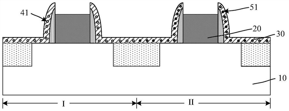
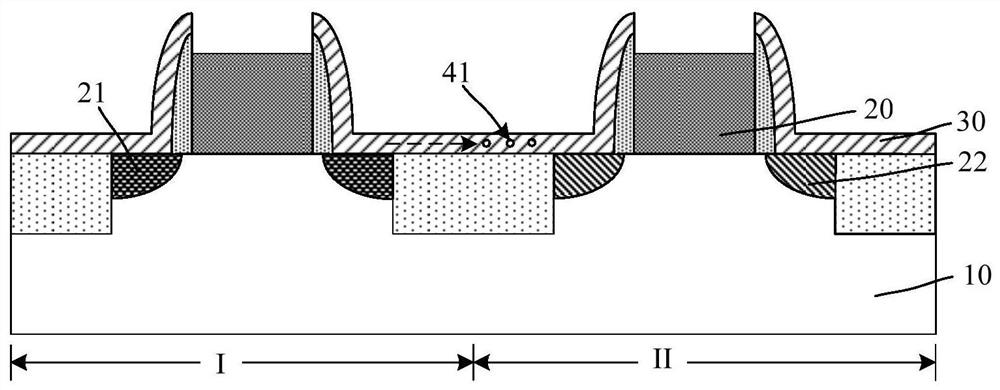
[0033] Combined reference figure 1 with figure 2 , Shows a schematic structural diagram corresponding to each step in a method for forming a semiconductor structure.

[0034] reference figure 1 , A substrate 10 is provided, the substrate 10 includes adjacent NMOS regions I and PMOS regions II; a gate structure 20 is formed on the substrate 10 of the NMOS region I and the PMOS region II; A polysilicon interconnection layer 30 is formed on the sidewalls of the structure 20 and the substrate 10 exposed by the gate structure 20; N-type ions 41 are doped into the polysilicon interconnection layer 30 of the NMOS region I; The polysilicon interconnect layer 30 is doped with P-type ions 51.

[0...


PUM


Abstract

The invention relates to a semiconductor structure and a formation method thereof. The method includes the following steps that: a substrate is provided, wherein the substrate includes an NMOS regionand a PMOS region which are adjacent to each other; gate structures are respectively formed at the NMOS region and the PMOS region on the substrate; a polysilicon interconnection layer is formed on portions on the substrate which are not covered by the gate structures; P type source-drain doped regions are formed in the substrate at two sides of the gate structure at the PMOS region; the polysilicon interconnection layer at the PMOS region is doped with blocking ions; and N type source-drain doped regions are formed in the substrate at two sides of the gate structure at the NMOS region after the polysilicon interconnection layer at the PMOS region is doped with the blocking ions. According to the semiconductor structure and the formation method thereof of the invention, the polysilicon interconnection layer at the PMOS region is doped with the blocking ions, so that N type ions can be prevented from diffusing into the PMOS region through the polysilicon interconnection layer when the Ntype source-drain doped region is formed, and therefore, the speed of a formed P type device can be improved.

Description

Technical field [0001] The present invention relates to the field of semiconductors, in particular to a semiconductor structure and a method of forming the same. Background technique [0002] With the gradual development of semiconductor process technology, the process size of semiconductor devices is getting smaller and smaller. [0003] Correspondingly, for MOS devices, the gate structure size, the active area (AA) size, and the contact hole plug (Contact, CT) size are also reduced accordingly. Therefore, in the manufacturing process of the semiconductor structure, after the source and drain doped regions and the gate structure are formed, the poly-interconnect is used to form the gate structure or the source and drain doped regions. Local interconnects can reduce the number of contact hole plugs, thereby reducing the process size of semiconductor devices. [0004] However, after the introduction of the polysilicon interconnection layer, the electrical performance of the formed s...

Claims


Application Information

Patent Timeline
Patent Type & Authority Patents(China)
IPC IPC(8): H01L21/8234H01L27/088
CPCH01L21/823475H01L27/088
Inventor 包小燕董天化葛洪涛王奇峰
Owner SEMICON MFG INT (SHANGHAI) CORP
Why Eureka
Try Eureka