A kind of power element encapsulation module and preparation method thereof
A technology for power components and packaging modules, applied in the field of power component packaging modules and their preparation, to achieve the effects of improving thermal conductivity and shock resistance, eliminating influence and improving thermal insulation performance
- Summary
- Abstract
- Description
- Claims
- Application Information
AI Technical Summary
Problems solved by technology
Method used
Image
Examples
preparation example Construction
[0029] The present invention also proposes a method for preparing the above-mentioned power element packaging module, which includes the following steps:
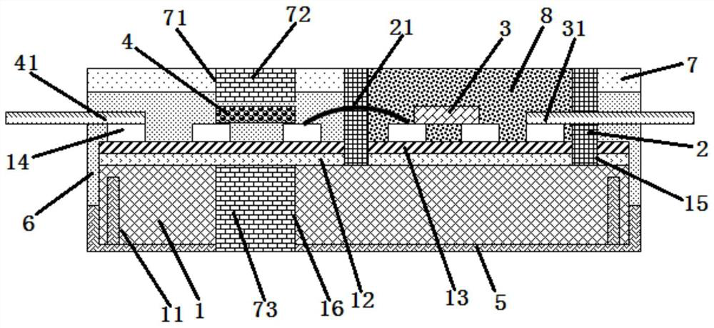
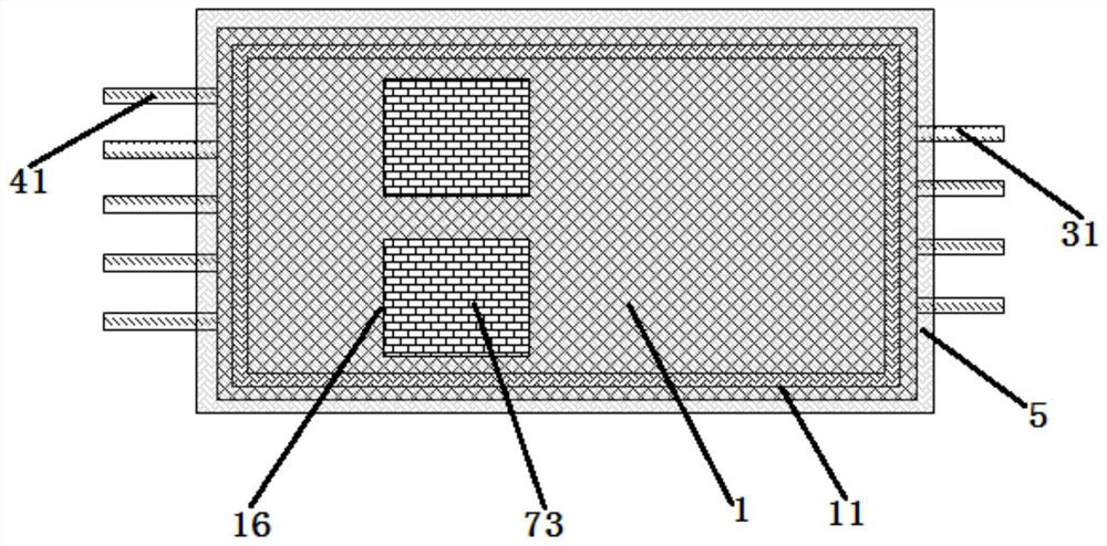
[0030] 1) A resin base is provided, and a first annular concave hole is formed on the peripheral edge of the lower surface of the resin base. The material of the resin base is one of PET, PEN, ABS, PMMA and PC, formed by a cutting process The first annular concave hole, the depth of the first annular concave hole is 1-1.5 mm, improves the tightness of the first heat-insulating sealant layer formed subsequently and the resin substrate, thereby improving the reliability of the entire power element packaging module. Sealing performance and moisture-proof performance;
[0031] 2) bonding a heat-conducting silica gel layer on the upper surface of the resin base to improve the heat conduction performance and shock resistance of the entire power element packaging module;
[0032] 3) Deposit an insulating material on the thermally...
Embodiment 1
[0041] The present invention proposes a method for preparing a power element packaging module, comprising the following steps:
[0042] 1) A resin base is provided, and a first annular concave hole is formed on the peripheral edge of the lower surface of the resin base. The material of the resin base is ABS, and the first annular concave hole is formed by a cutting process. The first The depth of the annular recess is 1.2 mm;
[0043] 2) bonding a heat-conducting silica gel layer on the upper surface of the resin base;
[0044] 3) Depositing an insulating material on the thermally conductive silica gel layer to form an insulating layer, depositing boron nitride by PECVD to form the insulating layer, and the thickness of the insulating layer is 100 microns;
[0045] 4) forming a circuit wiring layer on the insulating layer, the specific steps are: bonding copper foil on the insulating layer, and removing part of the copper foil through an etching process to form the circuit wi...
Embodiment 2
[0053] The present invention proposes a method for preparing a power element packaging module, comprising the following steps:
[0054] 1) A resin base is provided, and a first annular concave hole is formed on the peripheral edge of the lower surface of the resin base. The material of the resin base is PC, and the first annular concave hole is formed by a cutting process. The first The depth of the annular recess is 1.5 mm;
[0055] 2) bonding a heat-conducting silica gel layer on the upper surface of the resin base;
[0056] 3) Depositing an insulating material on the thermally conductive silica gel layer to form an insulating layer, depositing aluminum oxide by ALD to form the insulating layer, the thickness of the insulating layer is 150 microns;
[0057] 4) forming a circuit wiring layer on the insulating layer, the specific steps are: bonding copper foil on the insulating layer, and removing part of the copper foil through an etching process to form the circuit wiring l...
PUM
 Abstract
Description
Claims
Application Information

