DFB semiconductor laser

A laser and semiconductor technology, applied in the direction of semiconductor lasers, lasers, laser components, etc., can solve the problems affecting the reliability of lasers and the reduction of modulation bandwidth, and achieve the effect of increasing relaxation oscillation frequency, reducing parasitic capacitance, and improving modulation bandwidth

Pending Publication Date: 2022-03-29
HUAZHONG UNIV OF SCI & TECH
View PDF0 Cites 0 Cited by
  • Summary
  • Abstract
  • Description
  • Claims
  • Application Information

AI Technical Summary

Problems solved by technology

Using a buried heterojunction structure to reduce the width of the active region can effectively increase the modulation bandwidth, but the etching and oxidation of aluminum-containing materials close to the optical field will affect the reliability of the laser, especially the modulation bandwidth at high temperatures is significant Therefore, the industry generally adopts ridge waveguide lasers with simpler processes

Method used


Image

  • DFB semiconductor laser
  • DFB semiconductor laser
  • DFB semiconductor laser

Examples


Embodiment Construction

[0021] In order to make the object, technical solution and advantages of the present invention clearer, the present invention will be further described in detail below in conjunction with the accompanying drawings and embodiments. It should be understood that the specific embodiments described here are only used to explain the present invention, not to limit the present invention. In addition, the technical features involved in the various embodiments of the present invention described below can be combined with each other as long as they do not constitute a conflict with each other.

[0022] In the present invention, the terms "first", "second" and the like (if any) in the present invention and drawings are used to distinguish similar objects, and are not necessarily used to describe a specific order or sequence.

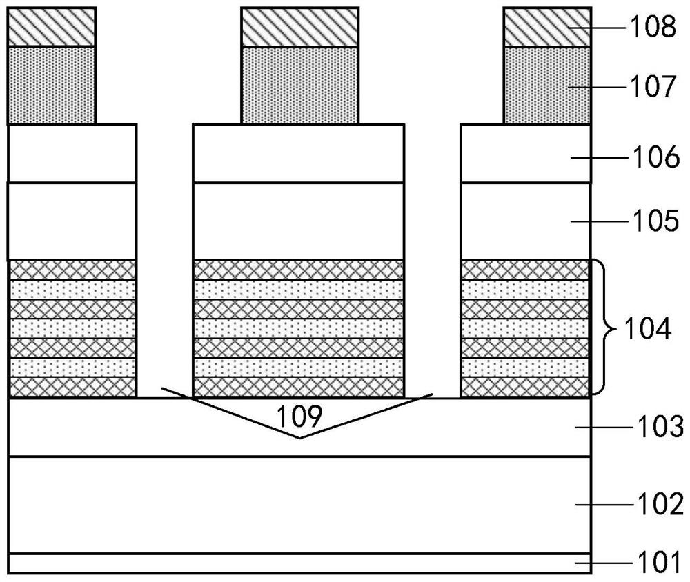
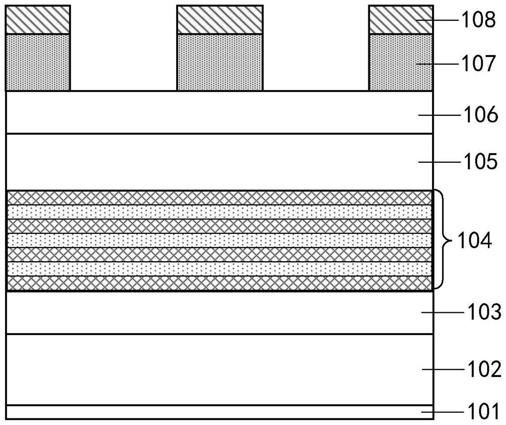
[0023] figure 1 A schematic structural diagram of a DFB semiconductor laser provided by an embodiment of the present invention. refer to figure 1 , combined wit...


PUM

PropertyMeasurementUnit
depthaaaaaaaaaa
widthaaaaaaaaaa

Abstract

The invention discloses a DFB semiconductor laser, and belongs to the field of semiconductor devices, the DFB semiconductor laser comprises an n-surface electrode, a substrate, an n-type lower cladding, an active region, a grating layer, a p-type upper cladding, a ridge waveguide and a p-surface electrode which are sequentially epitaxially grown from bottom to top, and the active region is of a multi-quantum well structure; groove regions which are symmetrical to each other are etched on the two sides of the ridge waveguide, and the groove regions penetrate through the active region and are used for improving the modulation bandwidth of the DFB semiconductor laser. At normal temperature, the double-trench region improves the relaxation oscillation frequency by improving a light field limiting factor and reduces parasitic capacitance, and at high temperature, the double-trench region improves the relaxation oscillation frequency by reducing carrier diffusion, so that the modulation bandwidth can be improved at both the normal temperature and the high temperature. The manufacturing process is simple, the groove area is far away from a light field, the reliability problem caused by etching of an aluminum-containing material is avoided, and the modulation bandwidth of the DFB semiconductor laser is improved on the basis that the performance and reliability of the laser are not affected.

Description

technical field [0001] The invention belongs to the field of semiconductor devices, and more specifically relates to a DFB semiconductor laser. Background technique [0002] Directly modulated semiconductor lasers have the advantages of low cost, small size, and mass production, and are widely used in low-cost optical fiber communications. With the increasing demand for data transmission rates and the huge demand of data centers, high-speed distributed feedback semiconductor lasers have become the core light source. However, the modulation bandwidth of distributed feedback semiconductor lasers is limited by laser parasitic constants, damping, and relaxation oscillation frequency, and the modulated output optical signal is accompanied by frequency chirp and other phenomena. In addition, as the temperature increases, due to the increase of Auger recombination, the threshold current of the laser increases rapidly, and the differential gain of the laser decreases rapidly, which...

Claims


Application Information

Patent Timeline
Patent Type & Authority Applications(China)
IPC IPC(8): H01S5/125H01S5/22H01S5/24
CPCH01S5/125H01S5/24H01S5/2205
Inventor 张敏明田琦刘德明韩宇
Owner HUAZHONG UNIV OF SCI & TECH
Why Eureka
Try Eureka